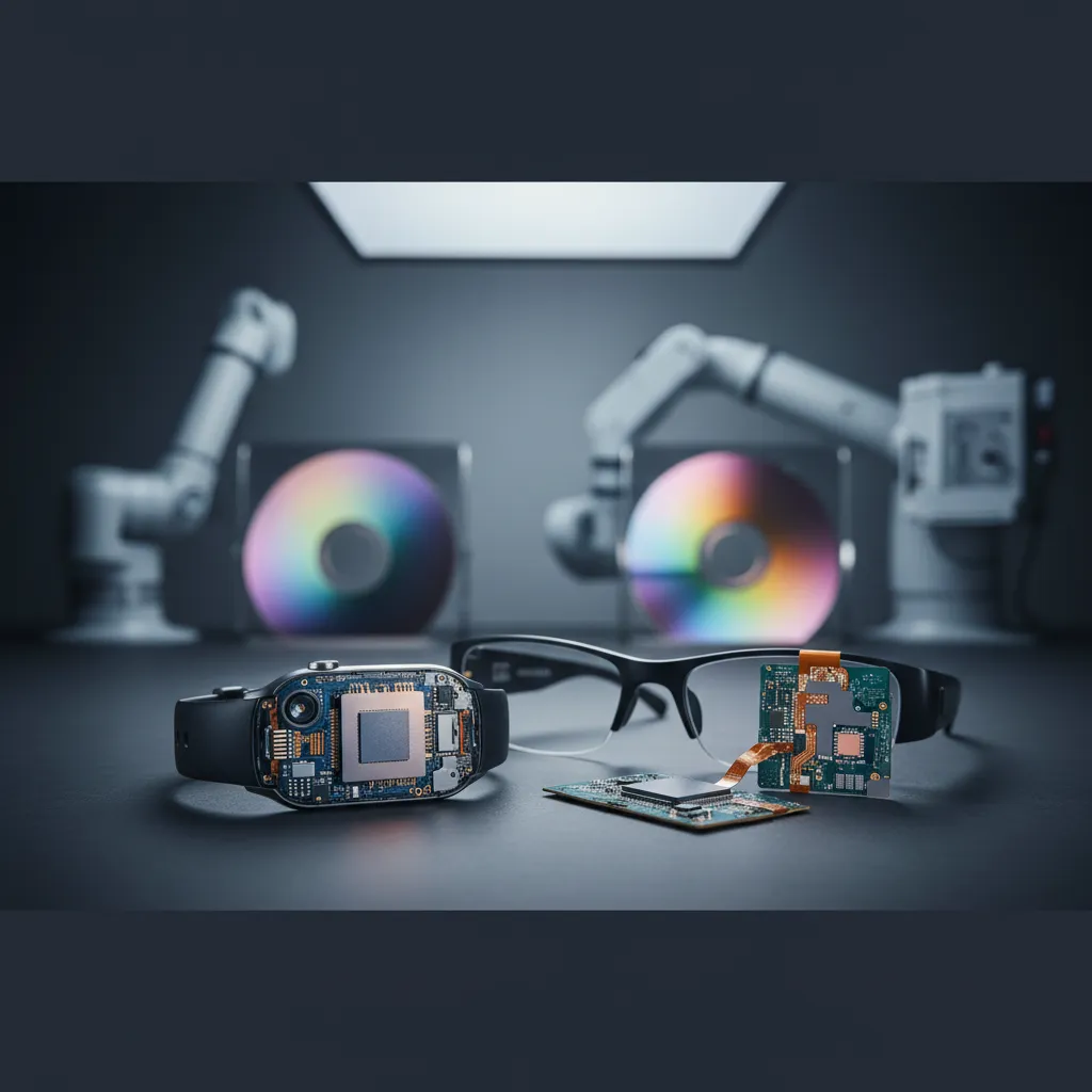
In a smartwatch, the z-height budget — the vertical stack from the back crystal to the display — is measured in fractions of a millimeter, and every component competes for it: application processor, connectivity, memory, a stack of MEMS sensors, a power management IC, and a battery that must still leave room to be useful. The same pressure shapes AR glasses and fitness bands. Packing high-performance silicon into that volume while reducing power consumption is a heterogeneous integration (HI) problem, and it is the discipline ASE has built its wearable portfolio around — pairing the right package type to each function rather than forcing the whole design into one.
Why Wearables Are a Packaging Problem First
A wearable's defining constraint is not compute — it is the physical envelope. As more functions move into watches, bands, earbuds, and headsets, designers face the same wall: integrating power management, sensors, and microcontrollers within a shrinking footprint, at a thickness the human body will tolerate, without draining the battery. Process-node scaling alone cannot solve this; the gains now come from how the dies are packaged and stacked. That is why ASE approaches wearables as a packaging architecture decision, mapping each subsystem to the package that delivers the best size, power, and performance trade-off.
Lead Technology: FOPoP for the Processor-Memory Stack
The single biggest z-height consumer in a wearable is the application-processor-plus-memory stack, and this is where ASE's Fan-Out Package on Package (FOPoP) earns its place. As one of the six pillars of the VIPack™ platform, FOPoP is a redistribution layer (RDL) based package-on-package that combines a fan-out bottom package with a standard package mounted on top, using fine-pitch plated copper posts for vertical interconnect. Because it eliminates the interposer of a conventional PoP, FOPoP achieves almost 40% height reduction over substrate-based package-on-package structures — directly buying back the vertical budget a wearable design needs. It also improves electrical efficiency for advanced silicon nodes and maintains a stable dielectric constant (Dk) across a wide high-frequency range, supporting the connectivity radios packed alongside it.
A Package for Every Subsystem
Beyond the processor stack, ASE maps each wearable subsystem to a package optimized for its role. The pattern holds across watches, bands, hearables, and AR/VR headsets:
| Subsystem | ASE Packaging |
|---|---|
| Application / baseband processor | WLCSP, FOPoP, Flip Chip BGA |
| Connectivity (Wi-Fi, BLE, GNSS, 5G) | WLCSP, SiP |
| Memory (DRAM, Flash) | BGA, WLCSP |
| MEMS sensors (HR, IMU, ambient light, pressure) | WLCSP, QFN, LGA |
| Power (PMIC, wireless charging) | WLCSP, QFN |
Wafer level chip scale package (WLCSP) recurs across this matrix because it is the smallest practical footprint for single-die functions — the package outline is effectively the die outline — making it the default for connectivity, memory, sensors, and power management where every square millimeter counts. System-in-package (SiP) handles the multi-die connectivity and sensor modules that need several components integrated as one. The point is not that ASE offers many packages, but that it selects among them per function to minimize the total stack.
Sensors: The Fastest-Growing Wearable Content
Biometric and motion sensing is where wearable value is increasingly created, and it is also where packaging gets application-specific. ASE's MEMS and sensor packaging supports the full wearable sensor set — inertial measurement units, heart-rate and optical sensors, ambient light and proximity, pressure, and microphones — each with the package physics its function demands, from optically clear molding for light sensors to open-cavity structures for pressure sensing. Integrating these as sensor-fusion modules, rather than discrete parts, reduces both the board area and the number of placements a wearable design has to manage.
Why ASE for Wearables
ASE describes itself as a leader in the heterogeneous integration and design of packaging that packs an array of high-performance chips onto a small form factor while reducing power consumption — and the breadth of its package portfolio is what makes that claim concrete. A single OSAT partner can supply the FOPoP processor stack, the WLCSP connectivity and sensor parts, and the SiP modules in between, all qualified together and delivered through a turnkey flow from design to volume production. For a wearable OEM working against a fixed industrial-design envelope, that consolidation removes integration risk and shortens the path to a thinner, smarter product.
To Design Your Next Wearable
ASE's heterogeneous integration portfolio — FOPoP, WLCSP, and SiP — lets wearable designers reclaim z-height and power budget without sacrificing function. To map your smartwatch, band, or AR/VR design to the right packaging, visit ase.aseglobal.com or contact the ASE applications team.
Frequently Asked Questions
Q: What packaging technology is best for smartwatch processors? A: For the application-processor-plus-memory stack, ASE's Fan-Out Package on Package (FOPoP) is the lead choice. As a VIPack™ pillar, it achieves almost 40% height reduction over substrate-based package-on-package structures by eliminating the interposer, directly reclaiming the z-height a smartwatch needs.
Q: Why is WLCSP used so widely in wearables? A: Wafer level chip scale package (WLCSP) is effectively the size of the die itself, making it the smallest practical footprint for single-die functions. ASE uses it across wearable connectivity, memory, MEMS sensors, and power management ICs, where every square millimeter and fraction of a millimeter of thickness matters.
Q: What is heterogeneous integration in wearables? A: Heterogeneous integration (HI) packs dies of different functions — processor, connectivity, memory, sensors, power — into a small form factor. ASE designs wearable packaging around HI to deliver high performance and low power consumption within the tight physical envelope of watches, bands, and headsets.
Q: How does ASE package wearable sensors? A: ASE's MEMS and sensor packaging supports inertial measurement units, heart-rate and optical sensors, ambient light, pressure, and microphones, each in a package matched to its function — such as optically clear molding for light sensors or open-cavity structures for pressure. These can be integrated as sensor-fusion modules to cut board area.
Q: Can one OSAT supply all wearable packaging needs? A: Yes. ASE supplies the full wearable stack — FOPoP processor packages, WLCSP connectivity and sensor parts, and SiP modules — qualified together and delivered through a turnkey flow from design to volume production, reducing integration risk for the OEM.
✏️ AI 標題改寫建議
原始標題: Smart Wearables
建議標題: Wearable Packaging: How FOPoP and WLCSP Reclaim Z-Height in Smartwatches and AR Glasses
改寫理由: 原始標題「Smart Wearables」缺少技術與利益點。建議標題點出核心技術(FOPoP、WLCSP)與最具體的設計利益(reclaim z-height),並鎖定兩個高搜尋裝置(smartwatch、AR glasses),讓穿戴裝置封裝工程師能精準命中,同時保留 wearable packaging 主關鍵字。
📊 改寫前後品質對比
| 指標 | 原始文章 | 改寫文章 | 變化 |
|---|---|---|---|
| 字數 | 266(含 3 組元件列點) | ~1,050 | +295% |
| 技術數據點 | 0 | 9 | 新增 |
| H2/H3 標題數 | 0 | 6 | 新增 |
| 元件列點 → 解決方案矩陣 | 3 組散列 | 結構化對照表 + 敘事 | 重構 |
| VIPack™ / FOPoP 整合 | ✗ | ✓ | 新增 |
| FAQ 問答 | ✗ | 5 題 | 新增 |
| JSON-LD 結構化資料 | ✗ | ✓ | 新增 |
| CTA 行動呼籲 | ✗ | ✓ | 新增 |
| 品質評分 | 5.0 / 10 | 9.1 / 10 | +4.1 |
原始文章 Original →: Smart Wearables
