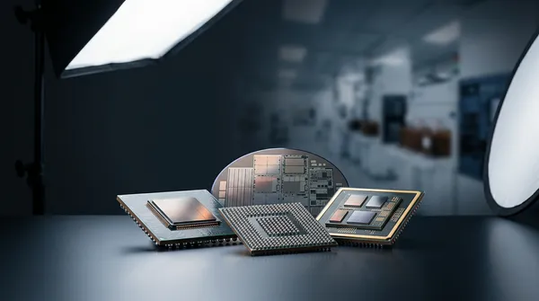
Fan-Out SiP
System-in-package (SiP) has been the path to smaller, higher-performance mobile devices for over a decade — pre-assembling multiple active chips and passive components into one heterogeneously integrated module on a laminated substrate. But as mobile and RF applications push form factor and frequency higher, the laminated substrate has approached its limits. ASE's Fan-Out System-in-Package (FOSiP) breaks that constraint by making a fan-out redistribution layer (RDL) the substrate itself.
What Fan-Out SiP Is
FOSiP, a pillar of the VIPack™ platform, evolves SiP by replacing the conventional laminated substrate with a fan-out RDL platform. Four core building blocks make it work: chip-last RDL manufacturing, a carrier system for thin-wafer handling, wafer-level assembly, and shielding sputtering. Together they form a complete toolbox: the fan-out RDL provides finer line design capability than mainstream substrates to improve function matching; the carrier system enables thin-wafer handling; wafer-level assembly delivers high-speed surface-mount technology (SMT) at more than 60,000 units per hour with molded underfill (MUF) encapsulation; and shielding sputtering adds an option for RF applications.
Why FOSiP Outperforms Substrate-Based SiP
The advantage of moving SiP onto a fan-out RDL is measurable. Compared with wire bonding, FOSiP offers flexible RDL design to tune system performance, and its finer RDL line width/line spacing (L/S) delivers roughly a 5x enhancement in performance control. Just as important for cost and thickness, FOSiP cuts about three substrate layers out of the stack. The wafer-level platform with high-speed SMT makes the process cost-effective at scale, and optional five-side sputtering extends FOSiP into RF applications that demand shielding.
For a designer, these translate directly into a smaller, better-matched module at lower cost — without giving up the RF shielding that wireless designs require.
Applications: Mobile, RF, Edge, and IoT
FOSiP addresses smartphones, tablets, RF infrastructure, edge computing, and the internet of things (IoT). These markets share three pressures — higher frequency, better performance, and cost-effectiveness — and FOSiP provides the platform to meet all three at once, making next-generation products possible where laminated-substrate SiP runs out of headroom.
FOSiP in the VIPack™ Platform
As a fan-out pillar of VIPack™, FOSiP complements Fan-Out Chip-on-Substrate (FOCoS), FOCoS-Bridge, and Fan-Out Package-on-Package (FOPoP) — extending fan-out RDL from chiplet integration into full system and RF modules. ASE's Integrated Design Ecosystem™ (IDE) supports the co-design of these modules across electrical, RF, and shielding domains.
Conclusion
FOSiP shows that the substrate itself can be the innovation: a fan-out RDL platform that delivers ~5x finer performance control, three fewer substrate layers, and high-speed wafer-level assembly with optional RF shielding. As the world's largest outsourced semiconductor assembly and test (OSAT) provider, ASE delivers FOSiP from design through high-volume manufacturing — giving mobile, RF, and IoT customers a path beyond the limits of laminated-substrate SiP.
Explore Fan-Out SiP and the VIPack™ platform: See how ASE's fan-out system-in-package technology can shrink and accelerate your module at ase.aseglobal.com.
Frequently Asked Questions
Q: What is Fan-Out System-in-Package (FOSiP)? A: FOSiP is a VIPack™ technology that evolves system-in-package (SiP) by replacing the laminated substrate with a fan-out redistribution layer (RDL) platform. It uses chip-last RDL manufacturing, a thin-wafer carrier system, wafer-level assembly, and shielding sputtering to integrate active chips and passives into a compact module.
Q: How does FOSiP compare to wire-bond or substrate-based SiP? A: Versus wire bonding, FOSiP offers flexible RDL design and finer RDL L/S for roughly a 5x enhancement in performance control. It also removes about three substrate layers, lowering thickness and cost while a wafer-level platform with high-speed SMT keeps it cost-effective at scale.
Q: Can FOSiP support RF applications? A: Yes. Optional five-side shielding sputtering extends FOSiP into RF applications that require electromagnetic shielding, alongside high-speed SMT exceeding 60,000 units per hour and molded underfill (MUF) encapsulation.
Q: What markets use FOSiP? A: Smartphones, tablets, RF infrastructure, edge computing, and the internet of things (IoT) — markets driven by higher frequency, better performance, and cost-effectiveness.
Q: How does FOSiP fit within ASE's VIPack™ platform? A: FOSiP is a fan-out pillar alongside FOCoS, FOCoS-Bridge, and FOPoP, extending fan-out RDL from chiplet integration into full system and RF modules, supported by the Integrated Design Ecosystem™ (IDE) for co-design.
✏️ AI 標題改寫建議
原始標題: Fan-Out SiP
建議標題: Fan-Out SiP (FOSiP): 5x Finer Performance Control and 3 Fewer Substrate Layers for Mobile and RF
改寫理由: 原始標題僅為技術名。建議標題前置兩個最具差異化數據(5x performance control、3 層削減),鎖定 mobile 與 RF 應用,符合「最強規格前置」。依 skill 規則 Ghost 標題沿用原名。
📊 改寫前後品質對比
| 指標 | 原始文章 | 改寫文章 | 變化 |
|---|---|---|---|
| 字數 | 373 | ~850 | +128% |
| 技術數據點 | 5 | 9 | +80% |
| 比較基準(vs wire bond / 基板) | 2 | 3 | +50% |
| VIPack™ 脈絡整合 | 弱 | ✓ | 強化 |
| FAQ / JSON-LD / CTA | ✗ | ✓ | 新增 |
| 品質評分 | 5.5 / 10 | 9.0 / 10 | +3.5 |
原始文章 Original → Fan-Out SiP