Fan-Out Panel-Level Packaging: How FOPLP Addresses the Interposer Size Barrier in AI Chip Integration
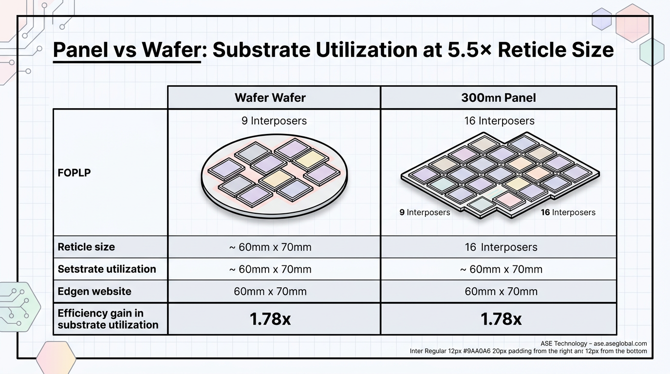
A 12-inch wafer accommodates just nine interposers at 5.5× reticle size — a utilization rate that makes advanced AI packaging economically unsustainable at scale. Fan-Out Panel-Level Package (FOPLP) technology offers a path forward, delivering 1.78× higher interposer output per substrate by transitioning from circular wafers to rectangular panels. ASE is actively developing FOPLP on a 310×310 mm automated production line, with a roadmap to 600×600 mm panels, to address the escalating packaging demands of AI accelerators and high-performance computing (HPC) systems.
This article examines ASE's FOPLP development within the VIPack™ platform — from the technical rationale behind panel-level processing to the specific challenges of scaling FOCoS and FOCoS-Bridge architectures beyond wafer boundaries.
Why AI Packaging Demands Larger Interposers
The advanced packaging architecture for AI and HPC positions high bandwidth memory (HBM) stacks in close proximity to AI processors — GPUs, AI ASICs — on a common interposer rather than on a printed circuit board (PCB). This configuration shortens the data path between compute and memory, enabling the bandwidth density and energy efficiency that large language model (LLM) training and inference workloads require.
As AI compute demand accelerates, interposer dimensions must grow to accommodate more chiplets in side-by-side configurations. ASE has achieved interposers at 3× reticle size today, but the roadmap extends to 3.5×, 4.5×, and 5.5× reticle dimensions. A 5.5× reticle interposer measures approximately 60 mm × 70 mm — larger than current mass-produced packaging substrates — creating a fundamental manufacturing challenge that conventional wafer-level processes struggle to address efficiently.
The Panel Advantage: 1.78× More Interposers per Substrate
Panel-level processing becomes compelling precisely where wafer-level processing falters — at large interposer sizes. The geometry tells the story: circular wafers waste material at the edges, and this waste grows disproportionately as interposer dimensions increase. A 300 mm wafer yields only 9 interposers at 5.5× reticle size. A 300 mm panel produces 16 interposers of the same dimension — a 1.78× efficiency gain.
For interposers exceeding 3× reticle size, the economic case for panel processing becomes decisive. The rectangular substrate eliminates edge waste, and the larger format enables higher throughput per processing cycle. This cost structure advantage is precisely what makes FOPLP essential for high-volume AI packaging, where each GPU or AI ASIC package requires the largest available interposer to integrate sufficient HBM capacity.
FOCoS and FOCoS-Bridge: Two Architectures Scaling to Panel
ASE's VIPack™ platform provides two primary fan-out architectures for AI chiplet integration, both of which are candidates for panel-level adaptation:
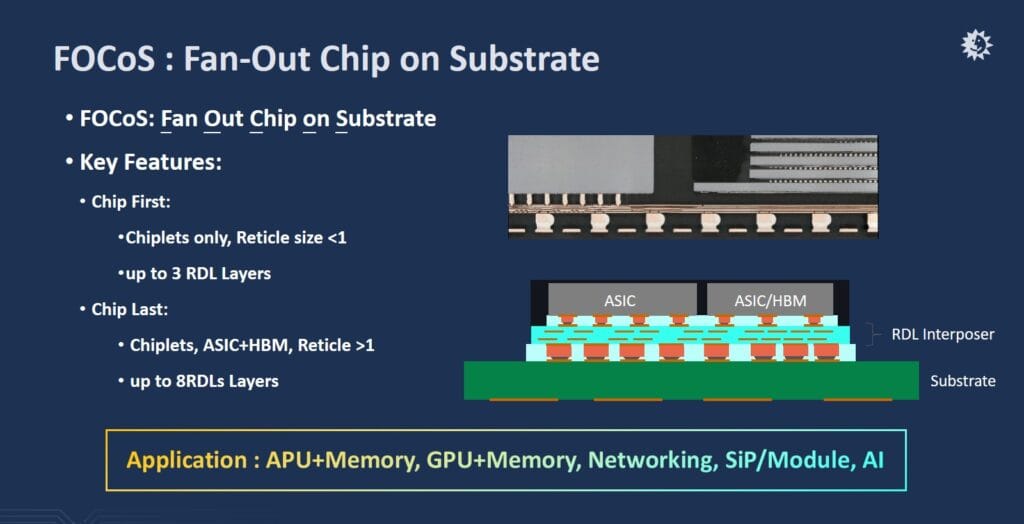
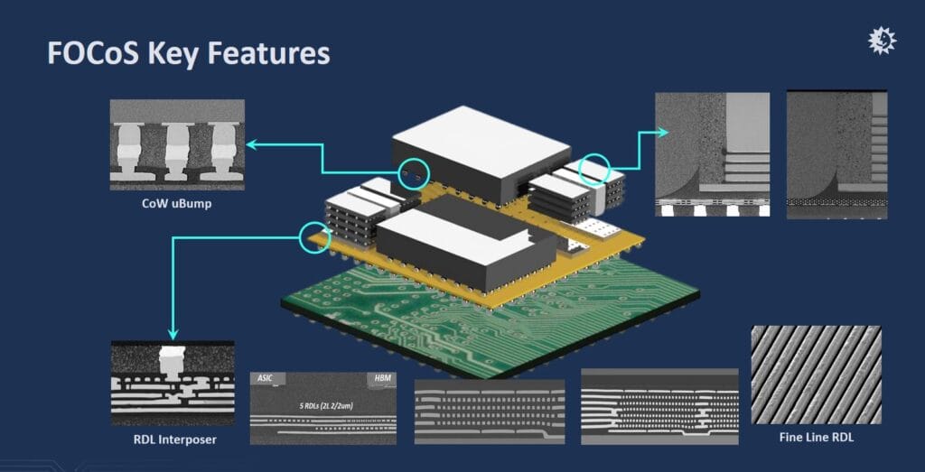
FOCoS — RDL-Based Chiplet Integration
Fan-Out Chip-on-Substrate (FOCoS) uses redistribution layer (RDL) interconnects to link chiplets on an organic interposer. Two variants serve different integration scales:
FOCoS-CF (Chip First) places dies directly onto a carrier before molding and RDL formation. This approach suits smaller integrations — typically 2–3 chiplets on interposers below 1× reticle size, using 2–3 RDL layers with line width/line spacing (L/S) at 2/2 μm.
FOCoS-CL (Chip Last) builds the RDL interposer first, then attaches chiplets via micro-bumps. This is the dominant approach for AI/HPC, supporting interposers exceeding 1× reticle size with up to 9 RDL layers — including at least 7 layers of fine-line routing at 2/2 μm L/S.
The scaling challenges are significant. μBump pitch on top-die ASICs has shrunk from 55 μm to 40 μm, trending toward 25–30 μm. HBM integration has evolved from 4-layer to 8-layer and 12-layer stacks, with interposer configurations growing from 4 HBMs to 8, with roadmaps extending to 12 and even 20 HBMs per package. Each HBM generation demands more RDL fine-line layers: HBM2/2E requires 2 layers of 2/2 μm L/S, HBM3/3E requires 4 layers, and HBM4/4E may need 8 RDL layers with 6 fine-line layers.
FOCoS-Bridge — Silicon Bridge for Ultra-Fine Interconnect
FOCoS-Bridge embeds silicon bridge dies within the fan-out RDL layer to provide ultra-fine interconnects (L/S < 0.5/0.5 μm) between chiplets — an order of magnitude finer than what RDL alone achieves. Because the bridge handles the highest-density routing, the surrounding RDL interposer requires only 5/5 μm L/S, significantly relaxing manufacturing requirements on the panel substrate.
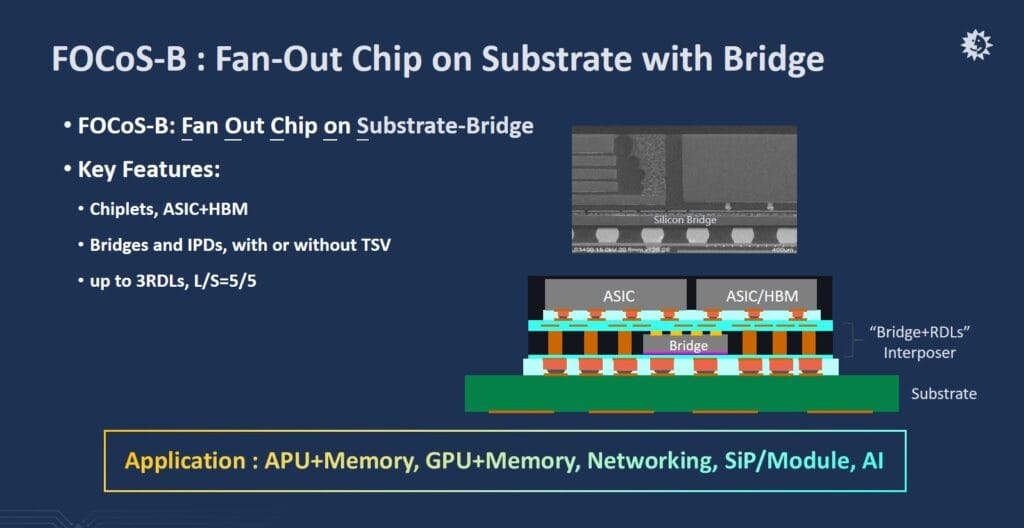
This architecture offers critical design flexibility: silicon bridges handle high-density die-to-die (D2D) communication while the interposer's wider-pitch RDL layers manage power delivery and signal routing. FOCoS-Bridge can also integrate independent integrated passive devices (IPDs) beneath the ASIC to enhance power integrity (PI) and signal integrity (SI).
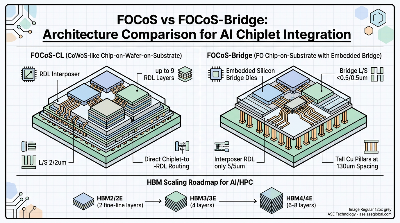
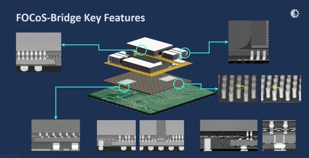
The challenges are equally demanding. FOCoS-Bridge requires dense arrays of tall copper pillars around bridge dies for vertical connections, with pillar spacing reduced from 150 μm to approximately 130 μm. Future bridge dies will incorporate through silicon via (TSV) structures for more efficient power delivery, and deep trench capacitors (DTCs) will be integrated into the interposer for enhanced PI/SI performance.
ASE's Panel-Level Development: 310×310 mm and Beyond
ASE is building an automated FOPLP production line starting with a 310×310 mm panel format. The strategy is pragmatic: begin with a manageable panel size to develop the process, then scale to 600×600 mm as manufacturing capabilities mature.
The transition from wafer to panel introduces fundamental process changes at every step:
Coating: Spin coating — the standard for wafer processing — cannot handle rectangular panels. ASE has transitioned to slit coating, which requires corresponding material reformulations to achieve uniform dielectric layer thickness across the panel surface.
Lithography: Interposers for AI chiplets typically exceed a single exposure field, requiring multi-reticle stitching in wafer lithography. For panel processing, maskless exposure technologies like Laser Direct Imaging (LDI) offer superior production efficiency and software-based compensation flexibility — eliminating mask constraints entirely.
Precision placement: With top-die micro-bump pitch at 35–40 μm, bridge die placement must achieve sub-micron accuracy. Cu studs at 20 μm diameter and PI vias at 10–15 μm leave minimal alignment margin — a challenge amplified by the larger thermal expansion variations inherent in panel substrates.
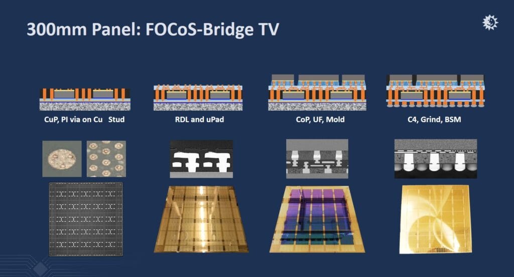
ASE's panel-level FOCoS-Bridge test vehicle, manufactured on a 300×300 mm panel, demonstrates the full process sequence: tall pillar formation and bridge die placement → molding and grinding → multi-layer RDL and μBump pad construction → chiplet attachment on 3× reticle-size interposers (~50 mm × 50 mm) → underfill, molding, carrier removal, and C4 bump formation.
The Collaborative Path Forward
FOPLP's complexity demands an ecosystem approach. No single company can independently overcome the combined challenges of panel-scale slit coating uniformity, maskless lithography accuracy, electroplating thickness control, and sub-micron placement precision on thermally expanding panel substrates. ASE is partnering with equipment manufacturers, material suppliers, and automation providers to build the FOPLP supply chain required for high-volume AI packaging production.
As AI workloads continue to drive interposer sizes beyond what wafer-level processing can economically support, FOPLP represents the manufacturing paradigm shift that enables continued scaling of heterogeneous integration (HI) — ensuring that packaging technology keeps pace with the relentless growth in AI compute demand.
To learn more about how ASE's VIPack™ fan-out packaging capabilities — including FOCoS, FOCoS-Bridge, and emerging FOPLP technology — can accelerate your next-generation AI and HPC designs, visit ase.aseglobal.com or contact our team to discuss your packaging requirements.
About ASE, Inc.
Advanced Semiconductor Engineering, Inc. (ASE), a member of ASE Technology Holding Co., Ltd. (NYSE: ASX, TAIEX: 3711) is the leading global provider of semiconductor manufacturing services in assembly and test. Alongside a broad portfolio of established assembly and test technologies, ASE is also delivering innovative VIPack™, advanced packaging, and system-in-package solutions to meet growth momentum across a broad range of end markets, including AI, automotive, 5G, high-performance computing, and more.
Frequently Asked Questions
Q: What is fan-out panel-level packaging (FOPLP)? A: Fan-Out Panel-Level Package (FOPLP) applies fan-out packaging processes to rectangular panel substrates instead of circular wafers. For large interposers exceeding 3× reticle size, panels deliver 1.78× more units per substrate than wafers, making FOPLP essential for cost-effective AI and HPC packaging at scale.
Q: How does FOCoS differ from 2.5D silicon interposer packaging? A: FOCoS uses redistribution layer (RDL) interconnects on an organic fan-out interposer, eliminating the need for a silicon interposer. This reduces cost and enables thinner packages while maintaining die-to-die routing at 2/2 μm L/S. FOCoS-Bridge adds embedded silicon bridges for sub-0.5 μm interconnects between critical chiplet pairs.
Q: Why are AI chip interposers getting larger? A: AI processors require increasing numbers of HBM stacks — evolving from 4 to 8, 12, and eventually 20 HBMs per package — to satisfy the bandwidth demands of large language model training. Each additional HBM expands the interposer's footprint, driving dimensions from 3× to 5.5× reticle size (approximately 60 mm × 70 mm).
Q: What are the main challenges in transitioning from wafer to panel processing? A: Key challenges include replacing spin coating with slit coating for rectangular substrates, adopting maskless lithography (such as LDI) for multi-reticle interposers, controlling electroplating uniformity across larger panel areas, and maintaining sub-micron bridge die placement accuracy despite greater thermal expansion on panel substrates.
Q: What is ASE's roadmap for FOPLP production? A: ASE is developing an automated FOPLP production line starting with 310×310 mm panels and plans to scale to 600×600 mm panels. The initial FOCoS-Bridge test vehicle on a 300×300 mm panel has demonstrated the full process flow, including 3× reticle-size interposers for AI chiplet integration.
Tags: Advanced Packaging, FOPLP, FOCoS, FOCoS-Bridge, VIPack, AI, HPC, Heterogeneous Integration, Panel-Level Packaging, Fan-Out Packaging