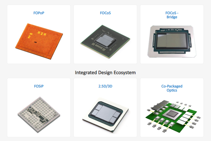
VIPack™: Six Packaging Pillars Engineered for the AI Compute Era
Patricia MacLeod — ASE, Inc.
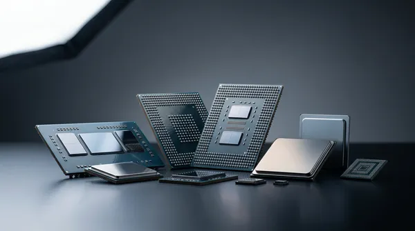
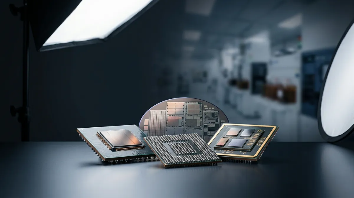
AI training clusters built on tens of thousands of GPUs now demand memory bandwidth exceeding 10 TB/s per accelerator, power delivery above 1,000 W per package, and die-to-die interconnect density that conventional organic substrates cannot achieve. These requirements have shifted advanced packaging from a back-end assembly step to the defining constraint — and opportunity — in next-generation system architecture. ASE's VIPack™ platform delivers the six technology pillars that address this challenge.
Why System-Level Integration Now Defines Semiconductor Performance
For decades, Moore's Law drove compute performance through transistor scaling within a single monolithic die. That approach is reaching its economic and physical limits. A 3 nm logic process offers diminishing returns per dollar, while AI workloads — with models now exceeding one trillion parameters — demand compute density, memory bandwidth, and energy efficiency gains that no single die can deliver alone.
Heterogeneous integration (HI) resolves this tension by partitioning system functions across specialized chiplets — logic, memory, I/O, photonics — and integrating them within a single package using advanced interconnect. The result is a system that combines best-in-node silicon from multiple process generations, achieving performance combinations that monolithic scaling cannot.
This architectural shift has placed the packaging platform at the center of the system design decision. The package is no longer passive interconnect; it is the integration engine.
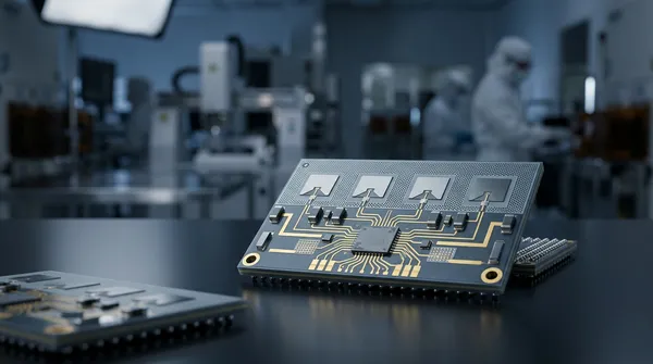
VIPack™: A Vertically Integrated Platform
VIPack™ is ASE's advanced packaging platform comprising six core technology pillars, supported by the Integrated Design Ecosystem™ (IDE 2.0) — a co-design framework that spans silicon, package, and system domains.
The name reflects both its structure and its scope: "VI" represents Vertically Integrated and the Roman numeral six, referencing the platform's six pillars. Each pillar addresses a distinct integration challenge, and customers select the 2–3 pillars most relevant to their architecture rather than adopting the full platform.
Pillar 1: FOPoP — Fan-Out Package-on-Package
FOPoP replaces conventional interposer-based package-on-package (PoP) structures with RDL-based vertical integration. The result: approximately 40% height reduction over substrate-based PoP, 3× shorter electrical paths, and up to 8× bandwidth density increase.
For mobile applications, FOPoP enables application processor and memory integration in z-height budgets measured in fractions of a millimeter. For networking and co-packaged optics (CPO), FOPoP achieves energy efficiency of 5 pJ/bit — down from 25 pJ/bit in conventional approaches — while supporting PIC, controller chips, laser, and fiber array unit integration with sub-micron passive alignment accuracy.
Pillar 2: FOCoS — Fan-Out Chip-on-Substrate
FOCoS mounts a fan-out package — with redistribution layer (RDL) interconnects at line width/line spacing (L/S) as fine as 2μm/2μm — onto a high-pin-count ball grid array (BGA) substrate. This eliminates the silicon interposer required by 2.5D approaches, reducing cost while maintaining short die-to-die (D2D) interconnects.
ASE offers three FOCoS variants tailored to different integration requirements:
- FOCoS-CF (Chip First): Chiplets connect directly to RDL through Cu vias — no micro-bumps between dies and fan-out RDL, achieving L/S 2/2 μm
- FOCoS-CL (Chip Last): Side-by-side chiplet configuration (ASIC + HBMs) connected through RDL and Cu micro-bumps at L/S 2/2 μm
- FOCoS-Bridge: Embedded silicon bridge dies with L/S 0.6/0.6 μm connecting ASIC to HBM within a fan-out RDL layer at L/S 10/10 μm
FOCoS supports packages with over 1,000 I/Os, targeting networking, server, HPC, and AI/ML applications. ASE's collaboration with Siemens on the FOCoS Assembly Design Kit (ADK) reduces package planning and verification cycles by 30–50% per design iteration.
Pillar 3: FOCoS-Bridge — Silicon Bridge Chiplet Integration
FOCoS-Bridge embeds tiny silicon bridge dies within the fan-out RDL layer to connect chiplets — such as GPUs and HBM — with ultra-fine-pitch interconnects. The silicon bridge achieves die-edge linear density (wire/mm/layer) an order of magnitude higher than conventional organic flip-chip packages.
Unlike 2.5D silicon interposer approaches, FOCoS-Bridge uses silicon only where two chiplets need connection, reducing cost and eliminating reticle-size constraints. The technology delivers electrical, signal, and power integrity comparable to full interposer solutions while enabling foundation for embedded passives and active die integration — including decoupling capacitors for power delivery optimization.
Pillar 4: FOSiP — Fan-Out System-in-Package
FOSiP integrates RF, analog, digital, and passive components within RDL layers, creating highly integrated system-in-package solutions. For mobile and edge AI applications, FOSiP streamlines RF design iteration and enables thinner form factors while addressing power delivery challenges at advanced silicon nodes.
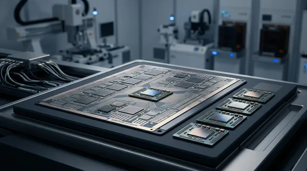
Pillar 5: 2.5D and 3D IC
ASE's TSV-based 2.5D and 3D IC packaging achieves ultra-high routing density with L/S down to 0.4/0.4 μm and I/O density exceeding 400 μbumps/mm². In 2.5D configurations, multiple active dies sit side-by-side on a silicon interposer; in 3D, dies stack vertically for the shortest interconnect and smallest footprint.
ASE pioneered the world's first mass production of 2.5D IC packages equipped with High Bandwidth Memory (HBM), establishing a production-proven foundation for AI accelerators, high-end GPUs, FPGAs, and network switches.
Pillar 6: Co-Packaged Optics (CPO)
As data-center networking evolves beyond 51.2 Tbps switch capacity, VIPack™ enables CPO integration by vertically combining electronic integrated circuits (EICs) with photonic integrated circuits (PICs). ASE's CPO solutions achieve energy efficiency below 5 pJ/bit — compared to 20–30 pJ/bit for conventional pluggable transceivers — with optical engine bandwidth scaling to 3.2–6.4 Tbps.
The IDE 2.0 Co-Design Advantage
Underpinning all six pillars is the Integrated Design Ecosystem™ (IDE 2.0), ASE's co-design framework that enables concurrent optimization across silicon, package, and system domains. IDE 2.0 addresses signal integrity, thermal performance, and power delivery network (PDN) design — reducing design iteration cycles and compressing time from architecture definition to high-volume manufacturing.
From Architecture to Volume: Why VIPack™ Matters for AI System Builders
The value of VIPack™ extends beyond individual technology pillars. For AI infrastructure architects, the platform provides three strategic advantages:
Architectural flexibility. Each AI workload has distinct packaging requirements. A large language model training accelerator demands maximum HBM bandwidth (FOCoS-Bridge or 2.5D IC), while an inference chip optimized for edge deployment may prioritize z-height and power efficiency (FOPoP or FOSiP). VIPack™ enables customers to select and combine pillars without re-qualifying a new packaging vendor.
Manufacturing scale. ASE operates the largest installed base of advanced packaging lines among OSATs, including 300 mm fan-out capacity. This scale translates to production readiness — customers avoid the 18–24 month qualification wait typically associated with new packaging platforms.
Design-to-production integration. IDE 2.0 connects chiplet architects with ASE's process engineers from day one, reducing the design-manufacturing handoff friction that delays time-to-market for multi-chiplet systems.
As AI drives unprecedented computational complexity and energy constraints, VIPack™ represents ASE's commitment to delivering the advanced packaging technologies required for the next generation of data-center and AI system integration — from architecture definition through high-volume manufacturing.
To explore how VIPack™ can accelerate your next-generation AI, HPC, or data-center design, visit ase.aseglobal.com/vipack or contact our team to discuss your packaging requirements.
About ASE, Inc.
Advanced Semiconductor Engineering, Inc. (ASE), a member of ASE Technology Holding Co., Ltd. (NYSE: ASX, TAIEX: 3711) is the leading global provider of semiconductor manufacturing services in assembly and test. Alongside a broad portfolio of established assembly and test technologies, ASE is also delivering innovative VIPack™, advanced packaging, and system-in-package solutions to meet growth momentum across a broad range of end markets, including AI, automotive, 5G, high-performance computing, and more.
Frequently Asked Questions
Q: What is VIPack™ and what does the name mean? A: VIPack™ is ASE's vertically integrated advanced packaging platform comprising six core technology pillars. The name combines "VI" for Vertically Integrated with the Roman numeral six, referencing the platform's six pillars: FOPoP, FOCoS, FOCoS-Bridge, FOSiP, 2.5D/3D IC, and co-packaged optics (CPO). Each pillar addresses a distinct heterogeneous integration challenge.
Q: How does FOCoS-Bridge differ from 2.5D silicon interposer packaging? A: FOCoS-Bridge embeds silicon bridge dies only where two chiplets need connection, while 2.5D uses a full silicon interposer spanning the entire package. FOCoS-Bridge delivers comparable electrical and signal integrity at lower cost, without reticle-size constraints. The bridge die achieves die-edge linear density an order of magnitude higher than organic flip-chip packages.
Q: What RDL line width/line spacing does VIPack™ support? A: VIPack™ supports a range of interconnect densities across its pillars. FOCoS and FOCoS-CF achieve L/S 2/2 μm for fan-out RDL. FOCoS-Bridge uses L/S 0.6/0.6 μm on the silicon bridge die. The 2.5D/3D IC pillar reaches L/S 0.4/0.4 μm with I/O density exceeding 400 μbumps/mm², representing the highest routing density in the platform.
Q: Which VIPack™ pillar is best for AI accelerator packaging? A: For AI accelerators requiring maximum HBM bandwidth, FOCoS-Bridge or 2.5D IC packaging are the primary choices — both enable tight coupling between GPU/ASIC dies and HBM stacks. For inference chips with edge deployment constraints, FOPoP or FOSiP provide optimized z-height and power efficiency. ASE's IDE 2.0 co-design framework helps customers select the optimal pillar combination for their specific architecture.
Q: How does VIPack™ support co-packaged optics for AI data centers? A: VIPack™'s CPO pillar integrates electronic and photonic ICs in a single package, achieving energy efficiency below 5 pJ/bit (compared to 20–30 pJ/bit for pluggable transceivers) with optical engine bandwidth of 3.2–6.4 Tbps. ASE offers two architectures: Photonic FOPoP (PIC on top) and Photonic 3D (PIC on bottom with TSV), supporting the transition from pluggable to co-packaged optics in next-generation AI clusters.
Tags: #VIPack #AdvancedPackaging #FOCoS #FOCOSBridge #FOPoP #FOSiP #3DIC #CPO #AI #HPC #HeterogeneousIntegration
Sources: - ASE VIPack™ Solution Page (ase.aseglobal.com/vipack/) - ASE FOCoS Solution Page (ase.aseglobal.com/focos/) - ASE FOCoS-Bridge Solution Page (ase.aseglobal.com/focos-bridge/) - ASE FOPoP Solution Page (ase.aseglobal.com/fopop/) - ASE 2.5D/3D IC Packaging Solution Page (ase.aseglobal.com/3d-ic-packaging/)