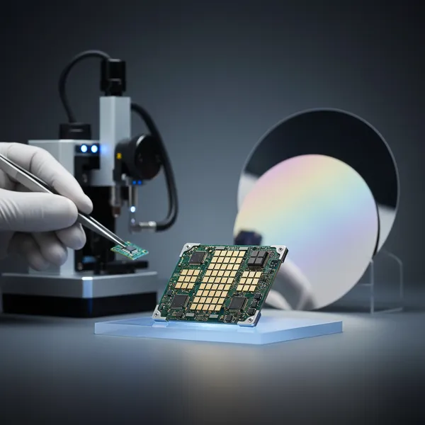
Antenna in Package
At millimeter-wave (mmWave) frequencies, every millimeter of trace between the radio and the antenna costs signal. A 28GHz beam that travels even a short distance across a printed circuit board (PCB) to reach a discrete antenna arrives attenuated, and the propagation losses only worsen as designs push toward 39, 60, and 77GHz. This is the constraint that makes the discrete-antenna approach — a printed shape on the PCB or a separate component placed near the transceiver — increasingly untenable for 5G and radar. Antenna in Package (AiP) answers it by integrating the antenna array directly into the IC package that carries the radio frequency (RF) transceiver, collapsing the interconnect between antenna and chip to package dimensions and recovering the signal that a board-level route would lose.
Why mmWave Forces the Antenna Into the Package
In 4G devices and sub-6GHz applications, antennas are manufactured discretely — printed on the PCB or assembled as an individual component near the RF front-end with a matching circuit. That works at lower frequencies, where wavelengths are long and routing losses are tolerable. mmWave changes the physics in ASE's favor: the antenna becomes small enough to fit inside the package, and the industry has moved to combine the transceiver and antenna in the same package precisely to position the radio closer to the antenna and boost the signal.
ASE develops AiP through its leadership in system-in-package (SiP) technology, and the integration delivers three concrete wins over a board-mounted antenna. The interconnect between antenna and RF chip shrinks, improving signal integrity and reducing the attenuation that otherwise undermines range and propagation at high frequencies. System-level design difficulty drops, giving product teams more flexibility and a faster path to market. And the package footprint stays small enough to fit 5G handsets and Internet-of-Things (IoT) endpoints where board area is scarce.
Three AiP Architectures, Matched to the Application
A typical flip chip ball grid array (FCBGA) AiP mounts the RF transceiver on the underside of the package substrate, connected to the main PCB through solder balls, with an antenna array formed on top of the substrate for transmission and reception. ASE uses flip-chip interconnect here specifically to mitigate interconnect loss between the RF chip and substrate. As a concrete reference design, ASE has built a 28GHz AiP in an FCBGA structure with a 2×2 stacked patch antenna array formed on a low-loss multilayer organic substrate.
| AiP architecture | Structure | Best fit |
|---|---|---|
| FCBGA-based AiP | RF chip flip-chip mounted under a BGA substrate; antenna array on top | 28GHz mmWave; reference 2×2 stacked patch array on low-loss organic substrate |
| AiP module | RF chip on a >12-layer antenna board; antenna array on the underside; FPC connector to handset mainboard | 5G smartphones routing multiple high-frequency signals |
| Hybrid-substrate AiP | RF chip on a BT substrate joined to an antenna flexible printed circuit (FPC) of low Dk/Df material | Designs prioritizing the lowest possible high-frequency signal loss |
The AiP module targets the smartphone: the RF chip sits on top of a multilayer antenna board, typically more than 12 layers, with the antenna array formed on the underside and a connector that carries multiple high-frequency signals to the phone's mainboard over a flexible printed circuit (FPC). The hybrid-substrate variant takes a different route, mounting the RF chip on a conventional BT substrate joined to an antenna FPC built from low dielectric constant (Dk) and low dissipation factor (Df) materials — the material choice that enables the lowest signal loss for high-frequency operation. The three are not redundant; each resolves a different balance of electrical performance, thermo-mechanical reliability, compactness, manufacturability, and cost.
Built on ASE's SiP and Heterogeneous Integration Platform
AiP is not a standalone process — it is an extension of ASE's heterogeneous integration (HI) capabilities. An AiP can be further integrated with front-end components such as power amplifiers (PA), low-noise amplifiers (LNA), switches, filters, and even a power management integrated circuit (PMIC) to form a complete antenna module using SiP technology. That SiP flow contributes double-side molding, selective molding, passive component integration, and electromagnetic interference (EMI) shielding — including ASE's conformal shielding (CFS), which achieves better than 99.9% shielding effectiveness (SE greater than 30dB) across 0.5–6GHz. For fan-out-based RF integration, AiP connects directly to Fan-Out System-in-Package (FOSiP), a pillar of ASE's VIPack™ advanced packaging platform, giving designers a route to denser antenna-module integration than a substrate-only build allows.
Measurement: Turning a Validated Design Into a Shipping Product
A mmWave antenna design is only as good as the team's ability to verify it. Over-the-air (OTA) testing of 5G beamforming antennas and validation of integrated arrays remain genuine engineering challenges, so ASE co-developed an AiP measurement system with Keysight Technologies to test AiP parameters with high accuracy and repeatability. The capability is concrete: a Compact Antenna Test Range (CATR) chamber for mmWave antenna measurement; S-parameter coverage spanning a PNA at 10MHz–67GHz, a VDI extension module at 67–115GHz, and a broadband frequency extender at 10MHz–110GHz; and probe stations supporting 8-inch wafer-level double-side measurement as well as panel-level double-side measurement up to 600mm × 600mm. For a customer, this is what shortens the gap between a promising simulation and a competitive product reaching the market on schedule.
Where AiP Goes Next
Because the antenna shrinks with frequency, AiP already spans a wide band of high-frequency applications: 60GHz radios and gesture radars, 77GHz automotive radar, 94GHz phased arrays, 122GHz imaging sensors, 300GHz wireless links, and 5G mobile networks at 28, 39, 60, 77GHz and beyond 90GHz. As 5G densifies and 6G research pushes into the sub-terahertz range, the pressure to place the antenna within microns — not millimeters — of the radio will only intensify. ASE's combination of three production AiP architectures, a full SiP and HI process toolkit, and a Keysight-grade measurement chamber gives mmWave product teams a single partner from system design through volume manufacturing.
Designing a 5G, radar, or mmWave product that needs the antenna and radio in one package? Explore ASE's Antenna in Package and system-in-package capabilities at ase.aseglobal.com.
Frequently Asked Questions
Q: What is Antenna in Package (AiP)? A: Antenna in Package is an antenna packaging solution that implements one or more antennas inside an IC package that also carries a bare RF transceiver chip. By integrating the antenna and radio in the same package, AiP shortens the interconnect between them, improving signal integrity and reducing the attenuation that limits range at millimeter-wave (mmWave) frequencies. It can be further integrated with PA, LNA, switches, filters, and PMIC into a full antenna module using ASE's system-in-package (SiP) technology.
Q: Why is AiP used for 5G and mmWave instead of a discrete antenna? A: At mmWave frequencies the antenna becomes small enough to fit inside the package, and integrating it with the transceiver positions the radio closer to the antenna to boost the signal. A discrete antenna printed on the PCB or placed as a separate component forces the high-frequency signal to travel farther and arrive attenuated. AiP collapses that path to package dimensions, addressing the range and propagation challenges that appear at 28GHz and above.
Q: What AiP architectures does ASE offer? A: ASE offers three. FCBGA-based AiP mounts the RF chip under a BGA substrate with an antenna array on top — including a reference 28GHz design with a 2×2 stacked patch array on low-loss organic substrate. The AiP module places the RF chip on a multilayer (typically >12 layer) antenna board with the array on the underside and an FPC connector to a handset mainboard. Hybrid-substrate AiP joins a BT substrate to an antenna FPC made of low Dk/Df material for the lowest high-frequency signal loss.
Q: What applications use Antenna in Package? A: AiP serves high-frequency applications including 60GHz radios and gesture radars, 77GHz automotive radar, 94GHz phased arrays, 122GHz imaging sensors, 300GHz wireless links, and 5G mobile networks operating at 28, 39, 60, 77GHz and beyond 90GHz.
Q: How does ASE test and validate AiP designs? A: ASE co-developed an AiP measurement system with Keysight Technologies for high-accuracy, high-repeatability over-the-air testing. It includes a Compact Antenna Test Range (CATR) chamber; S-parameter measurement using a PNA (10MHz–67GHz), a VDI extension module (67–115GHz), and a broadband extender (10MHz–110GHz); plus probe stations for 8-inch wafer-level and panel-level (up to 600mm × 600mm) double-side measurement.
✏️ AI 標題改寫建議
原始標題: Antenna in Package
建議標題: Antenna in Package (AiP): How Integrating the Antenna and RF Chip Cuts mmWave Signal Loss for 5G and Radar
改寫理由: 原始標題僅為技術名詞,無關鍵字延伸、無價值主張。建議標題保留核心詞 Antenna in Package (AiP) 以維持 SEO 連續性,並補入差異化機制(integrating the antenna and RF chip)、量化利益方向(cuts mmWave signal loss)與目標應用(5G and radar),提升搜尋點擊率與技術決策者閱讀意願。依 skill 規則,Ghost 文章標題沿用原始標題,本建議僅供編輯團隊參考。
📊 改寫前後品質對比
| 指標 | 原始文章 | 改寫文章 | 變化 |
|---|---|---|---|
| 字數 | ~930 | ~1,150 | +24% |
| 技術數據點 | 9 | 18 | +100% |
| H2 分段 | 7(產品頁式) | 5(敘事式) | 重構 |
| 架構對照表 | ✗ | 1(三種 AiP × 結構 × 適用) | 新增 |
| VIPack™ / SiP 平台定位 | 部分(連結) | ✓ 敘事整合(FOSiP、HI、CFS) | 強化 |
| FAQ 問答 | ✗ | 5 題 | 新增 |
| JSON-LD 結構化資料 | ✗ | ✓ | 新增 |
| CTA 行動呼籲 | 連結列 | ✓(含價值主張) | 強化 |
| 品質評分 | 6.3 / 10 | 9.1 / 10 | +2.8 |
原始文章 Original → Antenna in Package