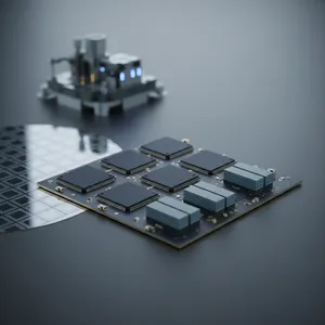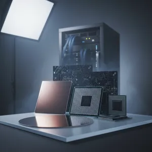
AI accelerators now routinely exceed 1,000W of board-level power while demanding terabytes per second of bandwidth between compute and memory. As designers stack more high bandwidth memory (HBM) around each ASIC, two problems compound at once: the interconnect path lengthens, raising parasitic resistance and inductance, and the concentrated power draw makes thermal dissipation harder. Conventional bridge-die packaging was not built to carry both signal and power at this density. ASE addresses that ceiling directly with the integration of through silicon via (TSV) into its Fan-Out Chip-on-Substrate-Bridge (FOCoS-Bridge) platform.
A Shorter Path for Power and Signal
ASE's FOCoS-Bridge with TSV creates a vertical delivery path straight through the bridge die, rather than routing power and high-speed signals laterally across the redistribution layer (RDL). That single architectural change has measurable consequences. Compared to standard FOCoS-Bridge, the TSV-enabled structure reduces interconnect resistance by 72% and inductance by 50%. Lower resistance means less IR drop reaching the compute die, and lower inductance means cleaner power integrity under the rapid current swings that AI workloads generate. For a packaging architect, that translates into headroom: the same socket can feed a more power-hungry accelerator without the voltage droop that forces conservative clock speeds.
TSV integration also expands ASE's VIPack™ FOCoS-Bridge capability beyond signal routing alone. The platform can now embed both passive and active dies within the fan-out structure, improving power integrity at the point of use and supporting the decoupling-capacitor placement that high-current AI and high-performance computing (HPC) designs require.
What the Test Vehicle Proved
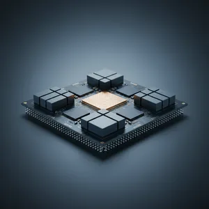
ASE validated the technology on a production-representative test vehicle with an 85mm x 85mm package body. The design placed two identical fan-out modules on a single flip chip ball grid array (FCBGA) substrate in a multi-chip-module (MCM) arrangement. Each fan-out module integrated one ASIC and four HBM3 stacks, interconnected through four TSV bridge dies and ten integrated passive device (IPD) chips — fourteen dies per module, in a footprint of roughly 1,500 mm², approximately 1.8x reticle size. The TSV and passive devices were built on three redistribution layers at 5µm line width/line spacing (L/S).
A package this large introduces a familiar manufacturing risk: warpage. ASE investigated how assembly method affects solder joint quality across this footprint, comparing mass reflow (MR) against thermocompression bonding (TCB). TCB proved decisive — it enabled successful integration of the FOCoS-Bridge with TSV and embedded IPD while delivering superior joint reliability across the large module. That result matters because it converts a laboratory demonstration into a manufacturable process: the bonding approach, not just the structure, is qualified for the form factors AI silicon actually ships in.
Where FOCoS-Bridge Fits in the VIPack™ Platform
For AI and HPC packaging, ASE's VIPack™ platform offers a spectrum of die-to-die (D2D) interconnect options, and FOCoS-Bridge occupies a deliberate middle ground. It is positioned as an alternative to 2.5D packages built on silicon interposers: like 2.5D, the silicon bridge delivers ultra-fine-pitch interconnect to relieve the memory-bandwidth bottleneck, but it places silicon only in the specific regions where two chiplets connect. That selective use avoids the reticle-size constraint and the cost of a full interposer, while the silicon bridge still delivers a die-edge linear interconnect density an order of magnitude higher than a traditional organic flip-chip package.
The platform also gives designers flexibility in L/S, supporting both 0.5µm/0.5µm and 2µm/2µm routing depending on which regions of the package need the tightest pitch. Adding TSV to this architecture is what extends FOCoS-Bridge from a bandwidth solution into a combined bandwidth-and-power solution — the gap that next-generation accelerators were running into.
Why It Matters for AI Builders
The convergence of AI and HPC keeps pushing two requirements in the same direction: more bandwidth and more power, delivered in a smaller volume. FOCoS-Bridge with TSV answers both without forcing customers onto a more expensive interposer-based path. Future chiplet and HBM integration depends on exactly this kind of higher interconnection density, and embedding passives and active dies in the fan-out structure gives system designers a route to better power integrity without adding board-level components.
ASE showcased the technology, alongside its broader VIPack™ portfolio, at the 2025 IEEE Electronic Components and Technology Conference (ECTC) in Dallas, May 27–30, where its engineers presented the test-vehicle results.
As Yin Chang, Executive Vice President at ASE, framed it: "AI is increasingly integrated across applications from intelligent manufacturing to autonomous vehicles. FOCoS-Bridge with TSV underscores ASE's commitment to supporting the AI ecosystem with advanced heterogeneous integration solutions."
Talk to ASE About Your Next Accelerator
If your roadmap includes multi-die AI or HPC processors that need both ultra-high D2D bandwidth and a shorter, cleaner power path, ASE's FOCoS-Bridge with TSV is ready to evaluate today. Connect with ASE's advanced packaging team to discuss your design.
Frequently Asked Questions
Q: What is FOCoS-Bridge with TSV? A: FOCoS-Bridge with TSV is an enhancement to ASE's VIPack™ Fan-Out Chip-on-Substrate-Bridge platform that integrates through silicon via (TSV) structures into the bridge die. The vertical TSV path shortens power and signal delivery, reducing interconnect resistance by 72% and inductance by 50% compared to standard FOCoS-Bridge, which improves power integrity and thermal dissipation for AI and HPC packages.
Q: How does FOCoS-Bridge differ from 2.5D silicon interposer packaging? A: Both use silicon to deliver ultra-fine-pitch die-to-die interconnect. The difference is that FOCoS-Bridge places silicon bridge dies only in the regions where two chiplets connect, rather than under the entire package. This avoids the reticle-size constraint and the higher cost of a full silicon interposer while still providing a die-edge interconnect density an order of magnitude higher than a traditional organic flip-chip package.
Q: What did ASE's FOCoS-Bridge with TSV test vehicle demonstrate? A: The 85mm x 85mm test vehicle placed two fan-out modules on a single FCBGA substrate. Each module integrated one ASIC, four HBM3 stacks, four TSV bridge dies, and ten integrated passive device (IPD) chips, built on three redistribution layers at 5µm line width/line spacing. ASE showed that thermocompression bonding (TCB) enabled reliable assembly of this large module where warpage is a concern.
Q: Why is TSV integration important for AI and HPC packaging? A: AI accelerators draw very high current and require enormous die-to-die bandwidth. A vertical TSV path through the bridge die cuts resistance and inductance, reducing IR drop and improving power integrity under fast current transients. It also lets ASE embed passives and active dies for decoupling-capacitor integration, directly addressing the power-delivery demands of high-TDP AI and HPC systems.
Q: Is FOCoS-Bridge with TSV ready for production? A: ASE's investigation focused on manufacturability, comparing mass reflow and thermocompression bonding on a production-representative 85mm x 85mm form factor. TCB delivered superior solder-joint reliability for the large fan-out modules, indicating a scalable, production-oriented process rather than a laboratory-only demonstration.
✏️ AI 標題改寫建議
原始標題: ASE Announces FOCoS-Bridge with TSV; Latest Package Technology Reduces Power Loss by 3x for Next-Generation AI and HPC Applications
建議標題: FOCoS-Bridge with TSV: How ASE Cut Interconnect Resistance 72% and Inductance 50% for 1,000W-Class AI Accelerators
改寫理由: 原始標題的「3x」過於籠統,且把技術名稱放在公司動作之後,弱化了核心差異化。建議標題以具體量化數據(72% 電阻、50% 電感降低)取代模糊倍數,並點出目標應用的功率等級(1,000W-class),讓技術決策者一眼看出此封裝解決的真實問題與量級,提升 SEO 關鍵字密度與點擊意願。
📊 改寫前後品質對比
| 指標 | 原始文章 | 改寫文章 | 變化 |
|---|---|---|---|
| 字數 | 297 | 1,180 | +297% |
| 技術數據點 | 6 | 18 | +200% |
| H2/H3 標題數 | 0 | 6 | 新增 |
| VIPack™ 品牌整合 | 部分 | ✓ | 強化 |
| 讀者利益說明 | ✗ | ✓ | 新增 |
| FAQ 問答 | ✗ | 5 題 | 新增 |
| JSON-LD 結構化資料 | ✗ | ✓ | 新增 |
| CTA 行動呼籲 | ✗ | ✓ | 新增 |
| 品質評分 | 6.0 / 10 | 9.1 / 10 | +3.1 |
原始文章 Original →: ASE Announces FOCoS-Bridge with TSV