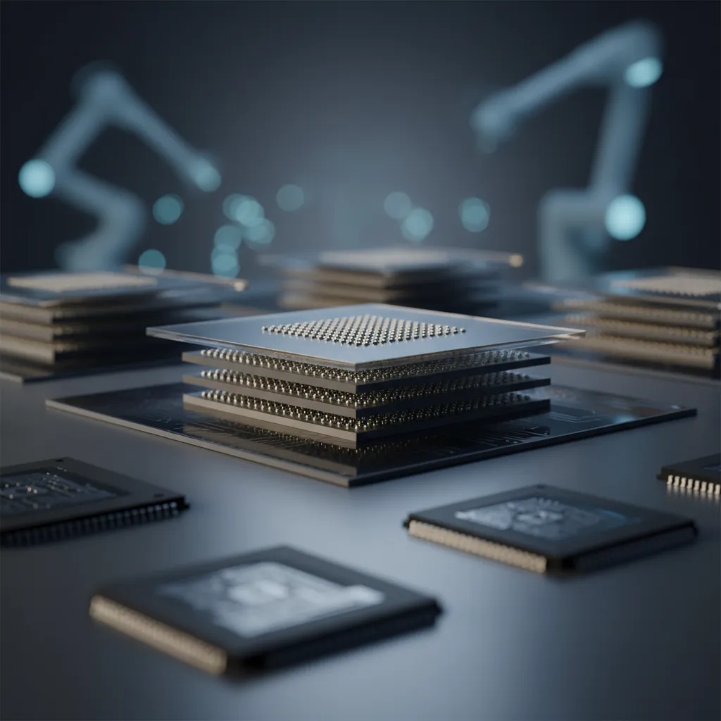
Flip Chip Packaging
Wire bonding can only place I/O around the perimeter of a die. Flip chip places it across the entire surface. By flipping the chip over and joining it to the substrate or leadframe with solder or gold bumps instead of bond wires, flip chip turns the die's whole face into an area array of interconnects — and in doing so removes the bond wire whose inductance limits high-frequency performance. That one structural change is why a flip chip package can carry up to 2,401 I/O in ASE's high-performance FCBGA, shrink the die for a given I/O count, and dissipate 6–8W through a heat spreader under natural convection. Flip chip is not a niche option at ASE; it is the interconnect foundation beneath FCBGA, FCCSP, and the wafer-level and fan-out platforms built on top of it.
Why Flip Chip Beats Wire Bonding Where It Counts
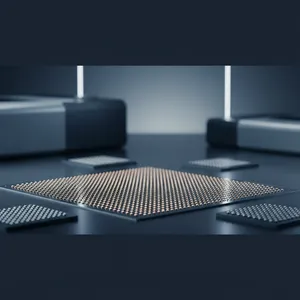
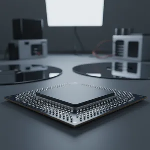
The name describes the method: the chip is flipped over to connect with the substrate or leadframe. Because the connection is made with solder or gold bumps rather than peripheral bond wires, the I/O pads can be distributed across the entire surface of the chip rather than only around its edge. Two consequences follow directly. The die can be made smaller for the same I/O count, and its circuit paths can be optimized. And with no bond wire in the signal path, signal inductance drops — the property that makes flip chip the better choice for high-frequency designs.
The benefits compound from there. All bonding for a flip chip package completes in a single process step, shortening assembly cycle time. The area-array pad layout raises I/O density, so designers either pack more I/O into the same die or shrink the die at constant I/O. The shorter path between die and substrate improves electrical performance. An external heat sink can attach directly to the chip for a direct thermal dissipation path. And the absence of wire and molding lets flip chip packages hold a lower profile. Underpinning all of it is wafer bumping — the essential process that forms the solder bumps before the wafer is diced — which ASE runs across 6-inch, 8-inch, and 12-inch wafers.
A Flip Chip Package for Every I/O and Reliability Target
ASE offers flip chip across four BGA families, each matched to a different combination of I/O count, body size, substrate, and ball pitch.
| Package family | I/O range | Body size | Substrate | Ball pitch |
|---|---|---|---|---|
| CCSP | 16–200 | 4×4 to 14.0×22.0mm | 2/4-layer laminate | 0.5–1.00mm |
| Ceramic FCBGA/PGA | up to 1,556 | 27×27 to 49.5×49.5mm | Ceramic | 0.8–1.27mm |
| FCBGA | 100–1,521 | 27×27 to 40.0×40.0mm | 2/4 laminate or 4–8 layer build-up | 1.0/1.27mm |
| HFCBGA | 256–2,401 | 12×12 to 52.5×52.5mm | 4–8 layer build-up | 1.0/1.27mm |
The range is what lets a customer match the package to the device rather than the other way around. A compact 200-I/O controller fits a chip-scale CCSP; a 1,500-I/O processor takes an FCBGA on build-up laminate; a high-reliability device destined for a CPU socket uses a ceramic FCBGA for its moisture resistance, electrical insulation, and higher thermal conductivity; and the most I/O-dense, thermally demanding parts move to the high-performance FCBGA at up to 2,401 I/O.
Three Offerings, Three Design Priorities
Flip Chip Chip Scale Package (FCCSP) targets devices at roughly 200 I/O or fewer. It delivers better chip protection and solder-joint reliability than direct chip attach (DCA) or chip on board (COB), performs comparably to known good die (KGD) while remaining far cheaper to test and burn in, and yields a thin, small, lightweight package — the right fit for cameras, DVD, voltage regulators, memory cards, and handsets.
Flip Chip BGA splits by substrate. The organic laminate or build-up version outperforms a wire-bond BGA in electrical performance, especially at high frequency, making it the choice for graphics, chipsets, and networking. The ceramic alumina version offers better moisture resistance, electrical insulation, and thermal conductivity than organic substrate, which is why it serves high-reliability commercial parts such as CPUs.
High Performance FCBGA (HFCBGA) composites an FCBGA with a heat spreader made of copper (Cu), aluminum (Al), or aluminum silicon carbide (AlSiC). The spreader extends the heat-conduction area by bonding to the rear of the silicon die, which desensitizes performance to chip size, lowers junction-to-case thermal resistance, and lets an external heat sink or fan work more effectively — producing 6–8W of dissipation under natural convection.
Tuning Performance: Molding and Heat Spreaders
Two enhancement options let ASE tune a flip chip package to its target. Overall molding, used on FCCSP, protects the chip and substitutes for underfill at lower cost while improving thermal performance and second-level reliability. A heat spreader, used on FCBGA, provides direct heat conduction by adhering to the rear side of the silicon chip — the mechanism behind the 6–8W of natural-convection dissipation in the high-performance family. The choice is application-driven: molding where cost and protection lead, a spreader where thermal headroom is the constraint.
Where Flip Chip Sits in ASE's Portfolio
Flip chip is foundational rather than terminal. The same area-array, bumped-die interconnect that defines a flip chip package is the building block beneath ASE's wafer-level packaging, fan-out, and system-in-package (SiP) platforms, and the wafer bumping that flip chip requires is the same process — including the Cu pillar route below 45μm pitch — that feeds ASE's broader turnkey line from substrate through final test. A customer adopting flip chip is not choosing a dead end; they are stepping onto the interconnect platform that heterogeneous integration is built on.
What Comes Next
As high-frequency and high-performance computing push I/O counts higher and thermal budgets tighter, flip chip's two structural advantages — area-array I/O density and a direct thermal path — only grow more valuable. ASE's four BGA families, spanning 16 to 2,401 I/O across laminate, build-up, and ceramic substrates, with molding and heat-spreader options on top, give product teams a flip chip path for nearly any electrical, thermal, and reliability target — backed by in-house wafer bumping across three wafer sizes.
Selecting a flip chip package for your next processor, RF, or networking design? Explore ASE's flip chip packaging and wafer bumping capabilities at ase.aseglobal.com.
Frequently Asked Questions
Q: What is flip chip packaging? A: Flip chip packaging flips the chip over and connects it to the substrate or leadframe using solder or gold bumps instead of bond wires. This lets I/O pads be distributed across the entire die surface as an area array rather than only around the perimeter, which shrinks the die for a given I/O count, optimizes the circuit path, and — by removing the bond wire — reduces signal inductance for better high-frequency performance.
Q: How is flip chip different from wire bonding? A: Wire bonding places I/O only around the perimeter of the die and adds a bond wire to each signal path. Flip chip uses an area array of solder or gold bumps across the whole die surface, completing all bonding in a single process step. The result is higher I/O density, a smaller die, shorter electrical paths, a lower package profile, a direct thermal dissipation path, and lower signal inductance.
Q: What flip chip packages does ASE offer? A: ASE offers four BGA families: CCSP (16–200 I/O, 0.5–1.00mm ball pitch), Ceramic FCBGA/PGA (up to 1,556 I/O on ceramic substrate), FCBGA (100–1,521 I/O on 2/4 laminate or 4–8 layer build-up), and high-performance HFCBGA (256–2,401 I/O on 4–8 layer build-up). It also offers FCCSP for devices around 200 I/O or fewer, organic and ceramic Flip Chip BGA, and heat-spreader HFCBGA.
Q: How does ASE manage heat in flip chip packages? A: ASE uses two enhancement options. Overall molding on FCCSP protects the chip, substitutes for underfill at lower cost, and improves thermal performance and second-level reliability. A heat spreader on FCBGA — made of copper (Cu), aluminum (Al), or aluminum silicon carbide (AlSiC) — bonds to the rear of the silicon die to extend the heat-conduction area, lowering junction-to-case thermal resistance and producing 6–8W of dissipation under natural convection.
Q: What applications use flip chip packaging? A: Flip chip serves consumer graphics and chipsets, microprocessors for PC and server, networking products including LAN, switching and transmission equipment, cellular base stations, and — through FCCSP — cameras, DVD, voltage regulators, high-speed memory cards, and handsets.
✏️ AI 標題改寫建議
原始標題: Flip Chip Packaging
建議標題: Flip Chip Packaging: Area-Array I/O up to 2,401 and 6–8W Heat-Spreader Cooling Across FCBGA and FCCSP
改寫理由: 原始標題僅為技術名詞。建議標題保留核心詞 Flip Chip Packaging,並補入最具差異化的量化能力(up to 2,401 I/O、6–8W 散熱)與主要封裝族(FCBGA、FCCSP),提升 SEO 點擊率與技術決策者辨識度。依 skill 規則,Ghost 文章標題沿用原始標題,本建議僅供編輯團隊參考。
📊 改寫前後品質對比
| 指標 | 原始文章 | 改寫文章 | 變化 |
|---|---|---|---|
| 字數 | ~650 | ~1,200 | +85% |
| 技術數據點 | 16 | 24 | +50% |
| H2 分段 | 3(含 Capabilities 列點) | 6(敘事式) | +100% |
| 封裝族對照表 | 散列 | 1(四族 × I/O/尺寸/基板/pitch) | 強化 |
| SiP / HI / bumping 平台定位 | ✗ | ✓ 敘事整合 | 新增 |
| FAQ 問答 | ✗ | 5 題 | 新增 |
| JSON-LD 結構化資料 | ✗ | ✓ | 新增 |
| CTA 行動呼籲 | ✗ | ✓(含價值主張) | 新增 |
| 品質評分 | 6.2 / 10 | 9.1 / 10 | +2.9 |
原始文章 Original → Flip Chip Packaging