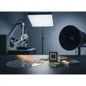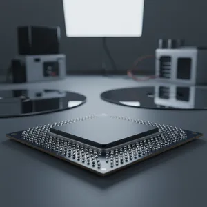
Two failure modes decide whether an advanced package survives qualification: it warps or cracks under mechanical and thermal stress, or it cannot shed heat fast enough and the junction overheats. Both get worse as packages grow larger, stack taller, and integrate more power-hungry silicon — and both are far cheaper to catch in simulation than after a build fails a temperature-cycling test. ASE's Stress-Thermal Laboratory exists to close that gap, combining numerical simulation, physical measurement, and pre-design analysis so customers see stress and thermal problems before committing to silicon.
The lab's value is in the sequence: model the behavior, measure the real part to validate the model, then fold both back into package and system design. Each stage feeds the next, which is why ASE treats stress and thermal as one discipline rather than two separate services.
Modeling and Simulation: Find the Failure Before the Build
The Stress-Thermal Laboratory characterizes package mechanical stress, thermal dissipation efficiency, and mold-flow behavior through numerical simulation, delivering a report customers use for evaluation before a part is built. The analyses run at two levels. At the package level, simulation predicts die crack and delamination and drives optimal design for low stress and high reliability. At the board level, it predicts the fatigue life of solder joints under the reliability tests that actually gate qualification — temperature-cycling test (TCT), drop test, and bending test among them.
Heat is the parallel challenge. Dissipating heat effectively from the chip is one of the hardest problems an engineer faces as power density climbs, so the lab provides both component-level and system-level thermal analyses. Its simulation scope covers the full set of mechanisms that move a package from "passes on paper" to "passes in the field":
- Thermal stress analysis — warpage, die stress, delamination
- System and board-level analysis — TCT, drop, bending
- Wire-bonding and wire-looping simulation
- Customized heat-sink effects
- Preliminary thermal studies for multi-chip module (MCM) and system-in-package (SiP)
- Hot-spot impact evaluations
- Transient analyses for power-pulse impacts
- Compact thermal models (CTMs) for system-level simulation
- Simulations for packages in sockets, under burn-in / HTOL test conditions
- Mold-flow prediction
Two of these matter especially for modern compute packaging: compact thermal models let a customer drop an accurate package thermal representation into a full system-level simulation without modeling every internal detail, and transient power-pulse analysis captures the bursty thermal loads that AI and high-performance computing (HPC) workloads impose — conditions a steady-state thermal number would miss.
Measurement: Validate the Model Against the Real Part
A simulation is only trustworthy once it is anchored to measured data, so the lab verifies package and system stress and thermal performance after a part is designed and built — and supports measurements at chip, package, and board level.
On the mechanical side, the measurement suite includes die-strength flexural measurement, wafer- and panel-level warpage measurement, stud-pull interface strength testing, material dog-bone tensile measurement, board- and system-level free-fall testing, die-pull measurement to evaluate under-bump metallization (UBM) and bump structural integrity, IC static-force compression testing, and solder-ball hot-bump-pull (HBP) strength testing. For board-level reliability, the lab runs the JEDEC and customized suite end to end: TCT, THD, drop, shock, bending, vibration, and twist.
On the thermal side, the lab measures the junction-resistance parameters that define how a package gives up heat, plus material conductivities:
| Parameter | What it characterizes |
|---|---|
| θJA | Junction-to-ambient thermal resistance |
| θJB | Junction-to-board thermal resistance |
| θJC | Junction-to-case thermal resistance |
| ΨJB | Junction-to-board thermal characterization parameter |
| ΨJT | Junction-to-top thermal characterization parameter |
These come with wind-tunnel testing for forced-convection thermal characterization, material thermal-conductivity measurements, and IC hot-spot analysis using thermal imaging — the data set that turns a thermal model from an estimate into a validated prediction.
Package/System Design and Analysis: Solve It Before the First Spin
The lab's third capability is the payoff of the first two. Drawing on a long-term, large database of package and board-level reliability, simulation, measurement, and customer co-design projects, ASE's Stress-Thermal Laboratory provides a pre-design solution — answering the stress and thermal questions before a package architecture is locked. This service covers warpage and component-stress prediction, package- and board-level reliability analysis, customized co-design and simulation at the system level, packaging material selection and structure design, and thermal optimal design for packages.
For the customer, this is the difference between discovering a warpage or hot-spot problem after a failed build and designing it out on the first spin. Material and structure choices made with measured-and-modeled data behind them are far more likely to pass qualification the first time — which is where the schedule and cost savings come from.
Where the Stress-Thermal Lab Fits in ASE's Portfolio
ASE is the world's largest outsourced semiconductor assembly and test (OSAT) provider, and the Stress-Thermal Laboratory is part of the analytical backbone that makes its packaging credible — alongside the electrical lab for signal and power integrity, and the broader test services organization. As designs move toward heterogeneous integration (HI), 2.5D/3D IC, and large multi-die bodies, warpage and thermal resistance become first-order design constraints rather than afterthoughts — and the same lab that validates a mature BGA also de-risks the most advanced packages ASE builds. Co-locating reliability and thermal engineering with assembly is what lets a customer treat them as design inputs from the start.
What Comes Next
As AI and HPC packages push toward higher power, taller die stacks, and larger substrate areas, the mechanical-stress and thermal-dissipation limits move to the center of package design. ASE's Stress-Thermal Laboratory — pairing simulation across warpage, fatigue, transient power, and mold flow with a full JEDEC reliability and thermal-resistance measurement suite, and feeding both into pre-design analysis — gives product teams a way to retire those risks before silicon, backed by a partner that carries the discipline from mature packages through heterogeneous integration.
Need to de-risk warpage, reliability, or thermal performance before you build? Explore ASE's Stress-Thermal Laboratory and lab services at ase.aseglobal.com.
Frequently Asked Questions
Q: What does ASE's Stress-Thermal Laboratory do? A: The Stress-Thermal Laboratory characterizes package mechanical stress, thermal dissipation, and mold-flow behavior through three linked capabilities: numerical simulation to predict failures before a build, physical measurement to validate models against real parts, and pre-design analysis that solves stress and thermal problems before a package architecture is locked. It works at chip, package, board, and system level.
Q: Which reliability tests can the lab simulate and measure? A: For board-level reliability, the lab covers temperature-cycling test (TCT), THD, drop, shock, bending, vibration, and twist — both in JEDEC-standard and customized forms. Simulation predicts solder-joint fatigue life and die crack/delamination under TCT, drop, and bending, while measurement validates those predictions on real assemblies.
Q: What thermal parameters does the lab measure? A: The lab measures junction-to-ambient (θJA), junction-to-board (θJB), and junction-to-case (θJC) thermal resistances, plus the junction-to-board (ΨJB) and junction-to-top (ΨJT) thermal characterization parameters. It also performs wind-tunnel forced-convection testing, material thermal-conductivity measurement, and IC hot-spot analysis with thermal imaging.
Q: Why simulate a package before building it? A: Warpage, die cracking, solder-joint fatigue, and overheating are far cheaper to catch in simulation than after a part fails qualification. ASE's lab models these behaviors, validates the models with measured data, then feeds the results into package and system design — so material and structure choices are made with evidence, raising the odds of passing qualification on the first spin and protecting schedule and cost.
Q: How does the lab support AI and HPC packaging? A: Two capabilities are especially relevant: transient power-pulse analysis captures the bursty thermal loads that AI and HPC workloads create — which steady-state numbers miss — and compact thermal models (CTMs) let customers drop an accurate package thermal model into full system-level simulation. Both help manage the warpage and thermal-resistance limits that dominate high-power, multi-die packages.
✏️ AI 標題改寫建議
原始標題: Stress and Thermal Lab
建議標題: Stress-Thermal Lab: How ASE Simulates and Measures Warpage, Solder-Joint Fatigue, and θJA Before Silicon
改寫理由: 原始標題僅為部門名稱,缺乏差異化與 SEO 關鍵字。建議標題保留核心詞 Stress-Thermal Lab,並補入最具搜尋意圖的能力點(warpage、solder-joint fatigue、θJA、before silicon),讓搜尋者與可靠度工程師一眼掌握該實驗室的價值主張。依 skill 規則,Ghost 文章標題沿用原始標題,本建議僅供編輯團隊參考。
📊 改寫前後品質對比
| 指標 | 原始文章 | 改寫文章 | 變化 |
|---|---|---|---|
| 字數 | ~452(列點堆疊) | ~1,150(敘事式) | 結構深化 |
| 技術數據點 | 散列、純列點 | 26(集中、含 θ 參數表) | 強化 |
| H2 分段 | 3(列點堆疊) | 5(敘事式) | 結構化 |
| simulate→measure→co-design 邏輯鏈 | ✗ | ✓ | 新增 |
| OSAT / HI / 跨實驗室定位 | ✗ | ✓ 敘事整合 | 新增 |
| FAQ 問答 | ✗ | 5 題 | 新增 |
| JSON-LD 結構化資料 | ✗ | ✓ | 新增 |
| CTA 行動呼籲 | ✗ | ✓(含價值主張) | 新增 |
| 品質評分 | 6.0 / 10 | 9.1 / 10 | +3.1 |
原始文章 Original → Stress and Thermal Lab