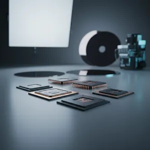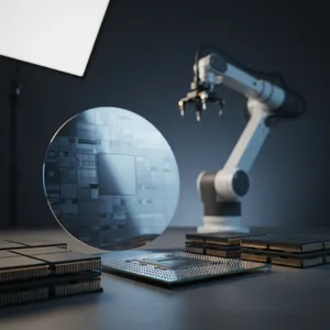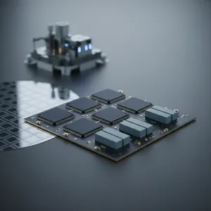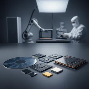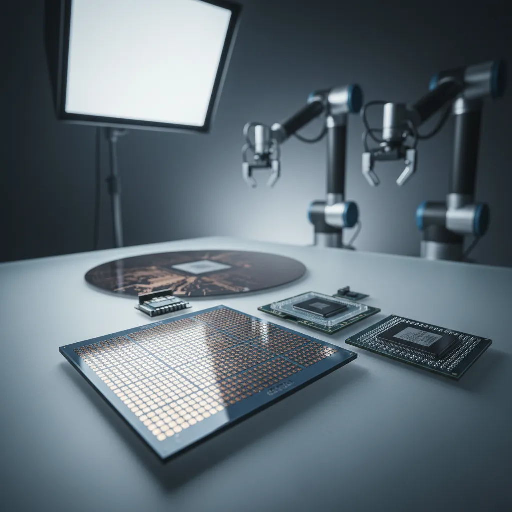
Every connected device in the data-centric era now ships against the same physical wall: more compute, sensing, and radio functions have to fit into a shrinking footprint while drawing less power. A smartwatch integrates an application processor, connectivity, memory, sensors, and a battery into a volume measured in cubic millimeters. An AI training rack places high bandwidth memory (HBM) within microns of a compute die to keep its tensor engines fed. A vehicle qualifies dozens of sensor and control packages to automotive-grade reliability. These are not the same problem — but they all push past what conventional single-chip packaging can deliver. As the world's largest outsourced semiconductor assembly and test (OSAT) provider, Advanced Semiconductor Engineering, Inc. (ASE) addresses each one with a packaging and test portfolio that spans wire bond to wafer-level integration to chiplet-class advanced packaging.
A Portfolio Organized Around End Markets
ASE's product strategy starts from the application, not the package. The semiconductor content behind data growth concentrates in a handful of demanding markets — AI, high-performance computing (HPC), edge data centers, 5G-to-6G communications, smart automotive, smart city, smart home, smart wearables, and smart hearables — and each market stresses a different axis of the design. AI and HPC are bandwidth- and power-bound. Mobile and wearable products are volume- and z-height-bound. Automotive is reliability- and temperature-bound. Rather than offer one packaging answer, ASE maps the right technology to each constraint, then delivers it as a turnkey service from design collaboration through high-volume manufacturing and final test.
VIPack™: Advanced Packaging for the Chiplet Era
For the most integration-intensive markets, ASE's VIPack™ platform provides the advanced-packaging building blocks that enable heterogeneous integration (HI) — combining dies of different process nodes, functions, and materials into a single package. VIPack™ comprises six technology pillars, and the value of the platform is that ASE selects among them rather than forcing every design into one architecture. Fan-Out Chip-on-Substrate (FOCoS) integrates chiplets on a fan-out substrate with redistribution layer (RDL) line width/line spacing (L/S) as fine as 2μm/2μm. FOCoS-Bridge connects heterogeneous dies through silicon bridges, achieving die-to-die interconnect density on the order of 200x that of conventional flip chip ball grid array (FCBGA). 2.5D/3D IC uses through silicon via (TSV) interposers for the tightest L/S, down to 0.5μm/0.5μm. Fan-Out Package on Package (FOPoP), Fan-Out System-in-Package (FOSiP), and Co-Packaged Optics (CPO) round out the platform for stacked mobile, sensor-fusion, and optical-interconnect designs respectively.
System-in-Package: Integration for the Connected Edge
Where advanced packaging serves the data-center and compute markets, system-in-package (SiP) serves the connected-edge markets — wearables, hearables, IoT, smart home, and automotive sensing. ASE defines SiP as a package or module containing a functional electronic system or subsystem, integrating processors, memory, surface-mount passives, filters, MEMS devices, and sensors through heterogeneous integration. The SiP toolbox is deep: conformal PVD shielding (CFS) that delivers electromagnetic interference (EMI) suppression above 99.9% — shielding effectiveness greater than 30dB across 0.5–6GHz — while cutting module area by 17% and thickness by 7% versus a metal can; compartment shielding (CPS) reaching 45–50dB across 1–6GHz in a barrier roughly 150μm thick; and high-density surface-mount technology (HD-SMT) placing 01005 passives at 3-mil component-to-component spacing. Together these let ASE shrink a multi-function module without sacrificing RF performance or yield.
Mapping Markets to Technology
The portfolio resolves into a clear set of market-to-technology pairings:
| Market | Primary Constraint | ASE Technology |
|---|---|---|
| AI / HPC | HBM bandwidth, >1,000W power | FOCoS-Bridge, 2.5D IC, powerSiP™ |
| 5G / 6G | mmWave RF, antenna integration | FOSiP, Antenna-in-Package, FOPoP |
| Smart Automotive | Reliability, thermal, sensor fusion | FOSiP, powerSiP™, MEMS/sensor packaging |
| Smart Wearables | Z-height, power, miniaturization | FOPoP, WLCSP, SiP |
| Smart Hearables / IoT | Form factor, RF shielding, sensors | SiP, conformal shielding, MEMS |
Each pairing reflects a specific engineering decision rather than a generic capability claim — FOPoP earns its place in wearables because it achieves roughly 40% height reduction over substrate-based PoP structures, and powerSiP™ earns its place in AI and automotive power stages because it raises current density from 0.4 A/mm² to 0.6 A/mm² while halving routing power loss.
Why ASE
ASE's differentiation is breadth plus scale. As the largest OSAT, it operates the broadest installed base of assembly and test capacity in the industry, and it couples that capacity with the Integrated Design Ecosystem™ (IDE) co-design platform so customers can validate package and system behavior before committing to tooling. For regulated markets, ASE holds the certifications those markets demand — including IATF 16949, ISO 26262, and AEC-Q100 for automotive. The result is a single partner who can take a design from early architecture exploration through qualification and volume production, compressing time-to-market across every application area data growth touches.
To Explore ASE's Application Solutions
ASE engineers packaging and test solutions for AI, HPC, 5G/6G, automotive, wearables, hearables, and the full range of connected applications. To find the right architecture for your product, visit ase.aseglobal.com or contact the ASE applications team.
Frequently Asked Questions
Q: What is the difference between SiP and advanced packaging? A: System-in-package (SiP) integrates a complete electronic subsystem — processors, memory, passives, and sensors — into one module, and is widely used in wearables, hearables, and IoT. Advanced packaging, such as ASE's VIPack™ platform (FOCoS, FOCoS-Bridge, 2.5D/3D IC), targets chiplet-class integration for AI and HPC where die-to-die bandwidth and fine line width/line spacing (L/S) down to 2μm/2μm matter most.
Q: Which packaging technologies does ASE use for AI and HPC? A: For AI and HPC, ASE applies FOCoS-Bridge for multi-die processors needing ultra-high die-to-die bandwidth, 2.5D IC with silicon interposer for integrating high bandwidth memory (HBM) stacks with compute dies, and powerSiP™ for power delivery, which raises current density from 0.4 A/mm² to 0.6 A/mm².
Q: What is heterogeneous integration? A: Heterogeneous integration (HI) combines dies of different process nodes, functions, or materials into a single package. ASE's VIPack™ platform enables HI through technologies like FOCoS-Bridge, which achieves die-to-die interconnect density roughly 200x that of conventional flip chip ball grid array (FCBGA).
Q: Does ASE support automotive-grade packaging? A: Yes. ASE manufactures automotive packaging under IATF 16949, ISO 26262, ISO 21434, AEC-Q100, and AEC-Q006 Grade 0+ certifications, serving ADAS, EV powertrain, sensor fusion, and infotainment applications with long-term tier-one supplier partnerships.
Q: What does turnkey OSAT service mean? A: A turnkey service means ASE handles the full flow — design collaboration through its Integrated Design Ecosystem™ (IDE), wafer bumping, assembly, module integration, and final test — under one partner, reducing qualification time and supply-chain risk for the customer.
✏️ AI 標題改寫建議
原始標題: Applications
建議標題: Advanced Packaging Across Every Market: How ASE Maps VIPack™ and SiP to AI, Automotive, and Wearables
改寫理由: 原始標題僅為單一導覽詞「Applications」,缺乏關鍵字與資訊量,對 SEO 與點擊率幾乎沒有幫助。建議標題納入核心品牌技術(VIPack™、SiP)與三大代表市場(AI、automotive、wearables),明確傳達「市場對應技術」的內容主軸,同時保留 advanced packaging 這個高搜尋量關鍵字,提升技術決策者的點擊意願。
📊 改寫前後品質對比
| 指標 | 原始文章 | 改寫文章 | 變化 |
|---|---|---|---|
| 字數 | 119 | ~1,150 | +866% |
| 技術數據點 | 0 | 16 | 新增 |
| H2/H3 標題數 | 0 | 7 | 新增 |
| VIPack™ 品牌整合 | ✗ | ✓ | 新增 |
| 市場對應技術表 | ✗ | ✓ | 新增 |
| FAQ 問答 | ✗ | 5 題 | 新增 |
| JSON-LD 結構化資料 | ✗ | ✓ | 新增 |
| CTA 行動呼籲 | ✗ | ✓ | 新增 |
| 品質評分 | 4.6 / 10 | 9.1 / 10 | +4.5 |
原始文章 Original →: Applications