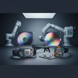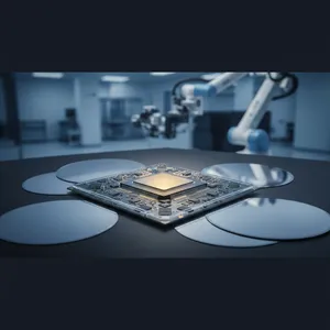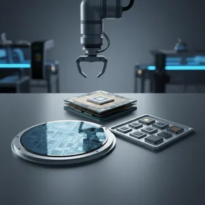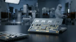
For decades, the semiconductor industry answered every demand for more performance with the same move: shrink the transistor and pack more onto a single monolithic die. That path is now stalling. Each new process node costs more to develop and yields less of an economic return, and forcing every function — logic, memory, RF, analog — onto one system-on-chip (SoC) compounds the cost and design complexity. Heterogeneous integration (HI) breaks this deadlock by assembling separately manufactured dies, each built on the process node best suited to its job, into a single high-functioning package. For IC designers, this is the difference between a multi-year monolithic re-spin and a modular package that reaches the market in a fraction of the time.
Why monolithic scaling no longer pays
The economics are straightforward. Packing more transistors onto a single chip becomes harder and more expensive at each node, and the largest SoCs now run into reticle-size limits and falling yields. Heterogeneous integration sidesteps that wall. Rather than fabricating one enormous die, ASE integrates multiple smaller dies — potentially from different nodes, foundries, and material systems — into one package that, in aggregate, delivers higher functional density and lower cost per function. The result is a continued increase in capability without the node-scaling penalty: higher performance, lower latency, smaller size, lighter weight, and lower power per function.
This is the core promise of HI as ASE applies it across three enabling technology families: system-in-package (SiP) for miniaturization and higher integration levels; 2.5D and 3D IC packaging for higher bandwidth and lower latency; and fan-in/fan-out wafer level packaging (WLP) for higher performance and density.
Chiplets: the modular answer to design cost
The chiplet model is the sharpest expression of the heterogeneous integration trend. Instead of designing one large chip on an expensive leading-edge node, designers partition the system into smaller, independently fabricated chiplets and reconnect them through die-to-die (D2D) interconnects inside the package. A typical chiplet architecture might combine CPU cores, memory ICs, and 3D-stacking technology to lift bandwidth and interconnect quality well beyond what a single die could economically achieve.
The payoff is in the design economics. Because chiplets reuse proven silicon and avoid committing every block to the most expensive node and fab process, they shorten design lead time and lower the cost threshold for entering advanced applications. That is why the approach has moved from novelty to mainstream in high-end processors, FPGAs, and networking ICs — domains where time-to-market and per-unit cost decide product viability.
Automating the design with APDK™
Heterogeneous integration adds parameters that traditional IC design flows were never built to handle: package-level redistribution, multi-die placement, warpage, and signal integrity across dissimilar materials. To give designers a robust, automated path through this complexity, ASE collaborated with Deca Technologies and Siemens Digital Industries Software to launch the APDK™ (Adaptive Patterning® Design Kit).
The APDK™ methodology provides a library of templates and extensive automation that guides the designer from initial layout, through Adaptive Patterning® simulation, to final sign-off using Siemens' Calibre software. For an engineering team, this means the iterative loop between package design and verification — historically one of the longest poles in an HI project — is compressed and made repeatable, reducing the risk that a layout decision surfaces as a manufacturing problem only after tape-out.
ASE's fan-out toolbox for chiplet integration
Volume manufacturing is where heterogeneous integration concepts either scale or stall, and ASE's experience in high-volume SiP production — including its M-series fan-out WLP technology — is what turns these architectures into shippable products. Within the ASE Technology Holding family, SPIL has developed a deep portfolio of fan-out packaging technologies purpose-built for chiplets, including Flip Chip Multi-Chip Module (FCMCM), 2.1D/2.5D/3D integration, Fan-Out Multi-Chip Module (FOMCM), Fan-Out Embedded Bridge (FOEB), and Embedded Multi-die Interconnect Bridge (EMIB).
The breadth matters because no single interconnect approach fits every design. A networking ASIC pairing with high bandwidth memory (HBM) has different bandwidth and reach requirements than a mobile application processor; having FOEB, FOMCM, and 2.5D/3D options under one roof lets ASE match the interconnect to the workload rather than forcing the workload onto a fixed packaging recipe. The high acceptance rate of these process technologies across customers is, in turn, what drives down manufacturing cost and improves speed to market.
Where this fits in VIPack™
These fan-out and 2.5D/3D building blocks are the foundation of ASE's VIPack™ platform — a vertically integrated advanced packaging platform that combines ultra-high-density interconnect, heterogeneous integration, and a co-design ecosystem. For chiplet-based designs, the most relevant VIPack™ pillars are Fan-Out Chip-on-Substrate (FOCoS), which builds shorter D2D interconnects on a redistribution layer (RDL) at line width/line spacing (L/S) as fine as 2μm/2μm, and FOCoS-Bridge, which embeds a silicon bridge die (L/S as fine as 0.6μm/0.6μm) to deliver interposer-class bandwidth without the reticle-size constraint of a full silicon interposer. For designs that need maximum routing density, the platform's TSV-based 2.5D/3D IC architectures reach L/S down to 0.4μm/0.4µm with over 400 µbumps/mm². Selecting among these is itself a design decision — and one ASE's co-design ecosystem is built to support.
The road ahead
Heterogeneous integration has moved packaging from a back-end afterthought to a strategic lever for system innovation. The combined R&D capacity of ASE, SPIL, and USI continues to widen the menu of SiP, fan-out, and chiplet options available to designers, while partnerships across the supply chain expand the application reach. For IC designers and system architects evaluating their next high-performance product, the practical takeaway is that the package is now a first-class design variable — and choosing the right HI architecture early is one of the highest-leverage decisions in the program.
Partner with ASE on your heterogeneous integration roadmap
Whether you are partitioning a monolithic SoC into chiplets or integrating HBM with a custom ASIC, ASE's SiP, fan-out, and 2.5D/3D portfolio — backed by the APDK™ design flow — can shorten your path from architecture to volume production. Explore ASE's heterogeneous integration solutions at ase.aseglobal.com to start the conversation.
Frequently Asked Questions
Q: What is heterogeneous integration in semiconductor packaging? A: Heterogeneous integration (HI) is the integration of separately manufactured components — dies on different process nodes, plus memory, passives, sensors, or MEMS — into a single higher-level assembly such as a system-in-package (SiP). Because each component is built on the process best suited to its function, the aggregate package delivers higher functional density and lower cost per function than forcing everything onto one monolithic chip.
Q: How are chiplets different from a traditional system-on-chip (SoC)? A: An SoC fabricates every function on one die at a single process node, which becomes expensive and yield-limited as designs grow. A chiplet design partitions the system into smaller dies that are fabricated independently — often on different nodes — and reconnected through die-to-die (D2D) interconnects inside the package. This reuses proven silicon, shortens design lead time, and lowers the cost threshold for advanced products.
Q: What is APDK™ and why does it matter for HI design? A: APDK™ (Adaptive Patterning® Design Kit) is a design kit ASE developed with Deca Technologies and Siemens Digital Industries Software. It provides templates and automation that carry a designer from initial layout through Adaptive Patterning® simulation to sign-off in Siemens' Calibre software, compressing the package design-and-verification loop that is typically one of the longest stages of a heterogeneous integration project.
Q: Which ASE technologies support chiplet integration? A: ASE and SPIL offer a broad fan-out toolbox including Flip Chip Multi-Chip Module (FCMCM), 2.1D/2.5D/3D integration, Fan-Out Multi-Chip Module (FOMCM), Fan-Out Embedded Bridge (FOEB), and Embedded Multi-die Interconnect Bridge (EMIB). Within the VIPack™ platform, FOCoS and FOCoS-Bridge are the primary RDL-based and silicon-bridge routes for chiplet-to-chiplet and chiplet-to-HBM interconnect.
Q: Why is heterogeneous integration considered essential to the future of computing? A: As monolithic transistor scaling delivers diminishing cost-performance returns, HI is the practical way to keep increasing functional density and reducing cost per function. It enables higher performance, lower latency, smaller form factors, and lower power per function — the requirements driving AI, 6G, edge and cloud computing, autonomous vehicles, and wearables.
✏️ AI 標題改寫建議
原始標題: Trends and Development in Heterogeneous Integration: Advancing the Smart Digital Age with System-in-Package and Chiplet Technologies
建議標題: Heterogeneous Integration Explained: How Chiplets and SiP Replace the Monolithic SoC — and Why ASE's APDK™ Design Flow Accelerates Time-to-Market
改寫理由: 原始標題偏向概論式、抽象("Advancing the Smart Digital Age"),缺乏具體技術對比與讀者利益。建議標題以「Heterogeneous Integration Explained」鎖定搜尋意圖,明確點出 chiplet/SiP 取代 monolithic SoC 的核心對立,並帶入 ASE 差異化資產(APDK™ 設計流程)與量化價值(time-to-market),提升 SEO 點擊率與技術決策者的閱讀動機。
📊 改寫前後品質對比
| 指標 | 原始文章 | 改寫文章 | 變化 |
|---|---|---|---|
| 字數 | 408 | 1,180 | +189% |
| 技術數據點 | 3 | 14 | +367% |
| H2/H3 標題數 | 0 | 7 | 新增 |
| VIPack™ 品牌整合 | ✗ | ✓ | 新增 |
| FAQ 問答 | ✗ | 5 題 | 新增 |
| JSON-LD 結構化資料 | ✗ | ✓ | 新增 |
| CTA 行動呼籲 | ✗ | ✓ | 新增 |
| 品質評分 | 5.8 / 10 | 9.1 / 10 | +3.3 |
原始文章 Original → : Trends and Development in Heterogeneous Integration: Advancing the Smart Digital Age with System-in-Package and Chiplet Technologies