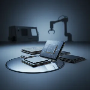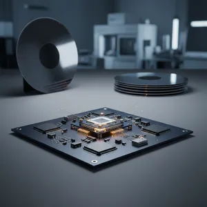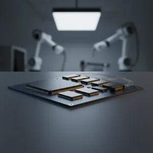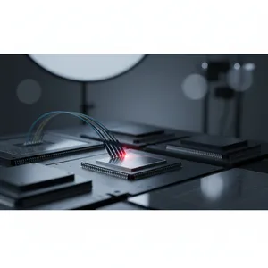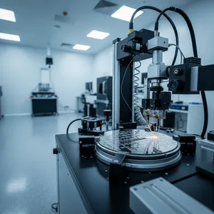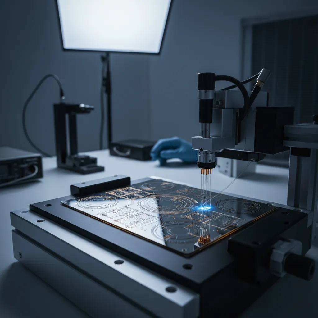
As AI and data-center traffic outgrow what copper interconnect can carry, the industry is shifting data movement from electrons to light — and that shift moves a hard problem onto the wafer. A silicon photonics (SiPh) photonic integrated circuit (PIC) can pass every electrical check and still be optically dead: a grating coupler misaligned by microns, an insertion loss out of spec, a polarization-dependent loss that closes the link. Committing an unverified PIC die into a co-packaged optics (CPO) module is expensive, so the die has to be proven good optically, at wafer level, before assembly. ASE's Optical Laboratory is built for exactly that — wafer-level (WL) optical test for SiPh products, plus optical thin-film characterization, modeling, and simulation.
The driver is the same one reshaping the rest of advanced packaging. As ASE's silicon photonics work describes, emerging Telecom/Datacom demand and high-performance computing (HPC) and artificial intelligence (AI) workloads are pushing toward light-based transmission for its higher bandwidth, lower latency over longer distance, lower power per bit, and higher package integration. To support SiPh product development against those targets, the Optical Lab developed a comprehensive optical test capability that meets the PIC where it is made — on 200mm and 300mm wafers.
Why Optical Test Moves to the Wafer
In a conventional electrical flow, wafer sort screens for known-good die before packaging. SiPh needs the optical equivalent. Among the technical building blocks ASE identifies for pluggable, on-board, and co-packaged optics is wafer-level optical probing test for known-good SiPh PIC die — the step that keeps a defective coupler or a lossy waveguide from being assembled into an optical engine that may later sit beside an ASIC. Catching it at the wafer is the difference between scrapping a die and scrapping a module.
That is why the Optical Lab pairs optical and electrical measurement in the same setup. A SiPh PIC is judged on both how light enters and exits and how the integrated photodetectors and modulators respond electrically, so the lab supports both optical-to-optical (O/O) and optical-to-electrical (O/E) testing on full 200/300mm photonics wafers.
Wafer-Level Optical Test
The core wafer-level capability characterizes the optical path end to end. The lab performs optical insertion loss (IL) and polarization-dependent loss (PDL) spectrum sweeps and photodetector (PD) responsivity measurement, the metrics that decide whether a link will close at the target data rate. Coupling light into a PIC is itself a measurement variable, so the lab runs grating coupler test across multiple incident angles — for example 8, 10, and 12 degrees — using either a single mode fiber (SMF) or a multi-channel fiber array unit (FAU) as the optical probe, which is what lets it move from single-channel characterization to the multi-channel coupling a real optical engine uses.
Behind the probe sits the instrumentation that sets the measurement range. A C-, L-, or O-band tunable laser covering 1240–1380nm and 1490–1640nm, equipped with a polarization synthesizer and a multi-channel optical power meter, lets the lab sweep across the wavelength bands SiPh products actually operate in and control polarization while doing so.
| Wafer-level optical test | Specification |
|---|---|
| O/O and O/E testing | 200mm / 300mm photonics wafers |
| Optical measurements | insertion loss (IL), polarization-dependent loss (PDL) spectrum sweep, PD responsivity |
| Grating coupler test | multiple incident angles (e.g., 8 / 10 / 12 deg.) |
| Optical probe | single mode fiber (SMF) or multi-channel fiber array unit (FAU) |
| Tunable laser | C/L/O-band, 1240–1380nm and 1490–1640nm, with polarization synthesizer |
The lab runs these in the configurations a SiPh product flow needs: O/O testing with SMF, O/E testing with SMF and a DC probe, and O/E testing with an FAU and DC probe cards. Moving between SMF and FAU coupling matters because a research measurement on one channel and a production measurement across many channels are different problems, and the Optical Lab is set up for both.
Optical Thin-Film Characterization and Simulation
Optical performance is not only about the waveguide; it is also about the films and structures light passes through. The lab's thin-film characterization, modeling, and simulation service measures transmittance and reflectivity, wavelength spectrum, and dimensions, and feeds those measurements into optical structure optimization. Pairing measurement with simulation lets the lab close the loop between what a film is specified to do and what it actually does — and adjust the structure before it reaches volume.
Where the Optical Lab Fits
ASE is the world's largest outsourced semiconductor assembly and test (OSAT) provider, and the Optical Laboratory is the analytical capability that makes its silicon photonics packaging testable. It works alongside the broader test services organization and the Electrical Laboratory, whose millimeter-wave and signal-integrity measurement complements optical characterization for mixed electrical-optical modules. As SiPh moves from pluggable transceivers toward on-board optics and CPO — where the optical engine is integrated next to the ASIC to shorten electrical paths and lower energy per bit — the ability to qualify a PIC die optically at the wafer becomes part of the same heterogeneous integration (HI) flow ASE uses to assemble those modules.
What Comes Next
Bandwidth demand from AI clusters and hyperscale data centers is what keeps pulling optics closer to compute, and each step closer raises the bar on testing the PIC before it is committed to a package. ASE's Optical Laboratory — wafer-level O/O and O/E test on 200/300mm wafers, IL/PDL and grating coupler characterization, C/L/O-band tunable-laser measurement, and thin-film characterization with simulation — gives SiPh product teams a way to prove a die good while it is still cheap to scrap, backed by the OSAT that will package it.
Developing a silicon photonics product that needs wafer-level optical test? Explore ASE's Optical Laboratory and full lab services at ase.aseglobal.com.
Frequently Asked Questions
Q: What does ASE's Optical Laboratory do? A: The Optical Lab provides wafer-level (WL) optical test for silicon photonics (SiPh) products, plus optical thin-film characterization, modeling, and simulation. It performs optical-to-optical (O/O) and optical-to-electrical (O/E) testing on 200mm and 300mm photonics wafers, measuring insertion loss, polarization-dependent loss, photodetector responsivity, and grating coupler performance.
Q: Why is wafer-level optical test important for silicon photonics? A: A silicon photonics PIC can pass electrical checks yet fail optically — through a misaligned grating coupler or out-of-spec loss. Wafer-level optical probing screens for known-good SiPh PIC die before assembly, so a defective die is caught at the wafer rather than after it has been built into an expensive co-packaged optics (CPO) module.
Q: What is the difference between O/O and O/E optical testing? A: Optical-to-optical (O/O) testing measures light in and light out — characterizing the optical path itself, such as insertion loss and coupling. Optical-to-electrical (O/E) testing measures the conversion between light and electrical signals, characterizing integrated photodetectors and modulators. ASE's Optical Lab supports both, including O/O with SMF, O/E with SMF and a DC probe, and O/E with a fiber array unit and DC probe cards.
Q: What wavelength range can the Optical Lab measure? A: The lab uses a C-, L-, or O-band tunable laser covering 1240–1380nm and 1490–1640nm, equipped with a polarization synthesizer and a multi-channel optical power meter. This spans the wavelength bands used by silicon photonics datacom and telecom products and supports insertion loss and polarization-dependent loss spectrum sweeps.
Q: How does the Optical Lab support co-packaged optics (CPO)? A: By qualifying the silicon photonics PIC die optically at the wafer, the Optical Lab provides the known-good-die step needed before a PIC is integrated into a CPO or on-board optics module. This fits ASE's heterogeneous integration flow, where the optical engine is packaged next to the ASIC to shorten electrical paths and reduce energy per bit.
✏️ AI 標題改寫建議
原始標題: Optical Lab
建議標題: Optical Lab: ASE's Wafer-Level Silicon Photonics Test — O/O and O/E, IL/PDL, and Grating Coupler Characterization
改寫理由: 原始標題僅為部門名稱,缺乏差異化與 SEO 關鍵字。建議標題保留核心詞 Optical Lab,並補入最具辨識度的能力(wafer-level SiPh test、O/O 與 O/E、IL/PDL、grating coupler),讓搜尋者與 silicon photonics/test 工程師一眼掌握該實驗室的價值主張。依 skill 規則,Ghost 文章標題沿用原始標題,本建議僅供編輯團隊參考。
📊 改寫前後品質對比
| 指標 | 原始文章 | 改寫文章 | 變化 |
|---|---|---|---|
| 字數 | ~218(列點 + 空標題) | ~1,150(敘事式) | 結構深化 |
| 技術數據點 | 列點 | wafer-level 能力表(含波長、角度、wafer size) | 強化 |
| H2 分段 | 2(含空 H3) | 5(敘事式) | 結構化 |
| known-good-die → CPO 價值鏈 | ✗ | ✓ | 新增 |
| OSAT / SiPh / HI 跨頁定位 | ✗ | ✓ | 新增 |
| FAQ 問答 | ✗ | 5 題 | 新增 |
| JSON-LD 結構化資料 | ✗ | ✓ | 新增 |
| CTA 行動呼籲 | ✗ | ✓ | 新增 |
| 品質評分 | 5.9 / 10 | 9.1 / 10 | +3.2 |
原始文章 Original → Optical Lab