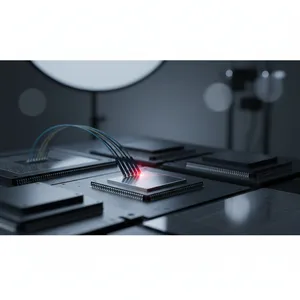
Butt-Coupling Optical Probe Card for Wafer-Scale Photonic-Integrated-Circuits Test with Polarization Control
A silicon photonics die only earns the label "known good" if it can be tested the way it will actually be used — and most photonic integrated circuits (PIC) ship coupled to fiber arrays at the chip edge, not through the top-surface grating couplers used on the wafer test floor. That mismatch is the gap an ASE team set out to close in a paper presented at the 2023 Conference on Lasers and Electro-Optics Europe & European Quantum Electronics Conference (CLEO/Europe-EQEC): a butt-coupling optical probe card that couples light to waveguide edges on the wafer, with polarization control, so a PIC can be screened before it is ever diced.
Why Wafer-Scale PIC Testing Is the Bottleneck for Silicon Photonics
Silicon photonics (SiPh) is moving data-center interconnect from copper to light because light delivers higher bandwidth at better energy efficiency — measured in pJ/bit — than electrical I/O can sustain at high speed. ASE's SiPh process flow already lists wafer-level optical probing test for known good SiPh PIC die as one of its key building blocks, alongside post-fab wafer-level bumping, high-accuracy laser die bonding, and 2.5D/3D integration of the electronic and photonic dies. The reason that probing step matters is economic: a co-packaged optics (CPO) module or on-board optics assembly integrates a photonic die next to expensive ASIC silicon, so shipping a defective PIC into that assembly wastes far more than the PIC itself.
Wafer-scale SiPh testing through grating couplers has matured. Coupled with image-processing alignment, the industry has demonstrated fully automated wafer-scale test platforms that bring an optical fiber down onto a top-surface grating and read the device out. The problem is what happens next. Most SiPh devices are eventually diced and packaged with fiber arrays through edge coupling — light enters the waveguide horizontally at the chip facet, not vertically through a grating. A device that passes a grating-coupler screen has not been tested in the optical configuration it will ship in. High-speed, on-wafer testing through edge coupling is therefore preferable, because it matches the final package.
The Hard Part: Coupling to a Waveguide Edge Without Dicing the Chip
Edge coupling on the wafer is difficult for a structural reason: the waveguide facet faces sideways, but on an intact wafer there is no exposed edge to couple into. Coupling light to the waveguide edges on-wafer, without first dicing the chip, is the critical enabling problem.
Several approaches to building optical probes for on-wafer edge coupling have been proposed. One obliquely cuts a planar lightwave circuit (PLC) chip; another uses a 3D-printing technique to form a lens-shaped structure at the end of a fiber tip. Both share the same operating principle — they redirect the guided wave from the top surface out into free space horizontally and illuminate the waveguide facet. Both also share the same drawback: fabricating these optical probes requires precision machining and assembly, which raises cost and limits how readily the probe can be scaled across a production test floor.
| Approach | Coupling principle | Practical limitation |
|---|---|---|
| Top-surface grating coupler probe | Vertical coupling through grating | Does not match the edge-coupled final package |
| Obliquely cut PLC chip probe | Redirect top-surface wave to facet | Requires precision machining/assembly |
| 3D-printed lens-on-fiber probe | Lens at fiber tip redirects to facet | Requires precision machining/assembly |
| Butt-coupling optical probe card (this work) | Direct edge coupling with polarization control | Test-floor-oriented probe-card form factor |
ASE's Approach: A Butt-Coupling Probe Card With Polarization Control
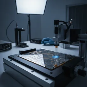
The ASE work takes a different route. Rather than redirecting light from the top surface, the butt-coupling optical probe card couples directly into the waveguide facet — butt-coupling places the fiber or coupling element end-on to the edge of the guide — and adds polarization control to the probe path. Polarization matters in SiPh because waveguide and grating responses are strongly polarization-dependent; a transverse-electric mode device behaves very differently under transverse-magnetic input. Controlling the input polarization at the probe is what makes an edge-coupled on-wafer measurement repeatable enough to screen against.
Packaging the coupling scheme as a probe card — the same form factor a test floor already uses for electrical wafer sort — is the practical move. It points the technique at automated, high-throughput wafer-scale testing rather than one-off lab characterization. The specific coupling loss, polarization extinction ratio, alignment tolerance, and throughput figures are reported in the original CLEO/Europe-EQEC paper [TBD - 待確認]; ASE's knowledge base does not restate these values, and they are not reproduced here to avoid fabricating data.
What This Means for a Silicon Photonics Customer
For a customer building CPO or on-board optics, the value is in the words "known good die." When a PIC can be edge-coupled and polarization-controlled on the wafer, the test result reflects how the part will perform after it is diced and attached to a fiber array — not an approximation through a grating coupler. That tightens the correlation between the wafer-sort screen and final-package behavior, which is exactly the correlation that lets a customer commit a photonic die to an expensive multi-die assembly with confidence.
It also keeps the screen at the wafer level, where it is cheapest. Catching a marginal PIC before dicing, before laser die bonding, and before integration next to an ASIC removes that defective die from the most costly part of the flow. For high-volume SiPh aimed at hyperscale data centers, high-performance computing (HPC), and artificial intelligence (AI) and machine learning workloads, a probe-card-based edge-coupling test is the kind of throughput-oriented capability that turns SiPh from a lab demonstration into a manufacturable product.
Where This Fits in ASE's Silicon Photonics Roadmap
This test capability sits within ASE's broader SiPh offering, which spans post-fab wafer-level processing, high-accuracy laser die bonding, 2.5D/3D packaging for electronic-IC/photonic-IC integration, and module assembly for pluggable, on-board, and co-packaged optics. As the industry pushes from 800Gbps pluggable transceivers toward 1.6T-class on-board optics and CPO, the number of photonic dies per system rises and the cost of an escaped defect rises with it. A wafer-scale, edge-coupled, polarization-controlled probe card is the screening layer that keeps that scaling economical.
What Comes Next
As SiPh volumes grow, on-wafer optical test has to look more like the final package and run at production throughput. A butt-coupling optical probe card with polarization control moves wafer-scale PIC testing in both directions at once — matching the edge-coupled package configuration and fitting the probe-card workflow a test floor already runs. By screening photonic dies the way they will actually be used, ASE helps its customers ship known-good silicon photonics into the AI and data-center systems that increasingly depend on light.
Bringing a silicon photonics or co-packaged optics design to volume? Explore ASE's silicon photonics and test capabilities at ase.aseglobal.com.
Frequently Asked Questions
Q: What is a butt-coupling optical probe card? A: A butt-coupling optical probe card is a wafer-test tool that couples light directly into the edge (facet) of a photonic integrated circuit (PIC) waveguide — placing the coupling element end-on to the waveguide — rather than coupling vertically through a top-surface grating. In ASE's CLEO/Europe-EQEC 2023 work, the probe card also includes polarization control, enabling repeatable on-wafer edge-coupled testing of silicon photonics (SiPh) devices before they are diced.
Q: Why test silicon photonics through edge coupling instead of grating couplers? A: Most SiPh devices are ultimately diced and packaged with fiber arrays through edge coupling, where light enters the waveguide horizontally at the chip facet. Testing on-wafer through edge coupling matches that final optical configuration, so the wafer-sort result better predicts how the device will behave in its shipped package — unlike a top-surface grating-coupler screen, which tests a different coupling path.
Q: Why is polarization control important in optical wafer testing? A: Silicon photonics waveguides and grating structures respond differently to transverse-electric and transverse-magnetic polarization states. Without control of the input polarization, an edge-coupled measurement is hard to reproduce. Adding polarization control to the probe card makes the on-wafer test repeatable enough to use as a production screen.
Q: Why does wafer-scale PIC testing matter for co-packaged optics? A: Co-packaged optics (CPO) and on-board optics integrate a photonic die next to costly ASIC silicon. Shipping a defective PIC into that assembly wastes far more than the PIC alone. Screening for known good die at the wafer level — before dicing, laser die bonding, and integration — removes marginal devices at the cheapest point in the flow.
Q: How does this test capability fit into ASE's silicon photonics services? A: ASE lists wafer-level optical probing for known good SiPh PIC die as a key building block alongside post-fab wafer-level bumping, high-accuracy laser die bonding, 2.5D/3D electronic-IC/photonic-IC integration, and module assembly. A butt-coupling, polarization-controlled probe card strengthens the wafer-level screening layer that supports pluggable, on-board, and co-packaged optics for data center, HPC, and AI applications.
✏️ AI 標題改寫建議
原始標題: Butt-Coupling Optical Probe Card for Wafer-Scale Photonic-Integrated-Circuits Test with Polarization Control
建議標題: Edge-Coupled, Not Diced: How ASE's Butt-Coupling Probe Card Screens Silicon Photonics Wafers the Way They Ship
改寫理由: 原始標題為會議論文式命名,技術詞彙正確但偏冗長、缺少讀者利益與差異化。建議標題以「Edge-Coupled, Not Diced」點出核心差異(在不切割晶圓的前提下做 edge coupling 測試),保留 silicon photonics、probe card 等關鍵字,並帶出對客戶的價值(以出貨時的耦合方式篩選 known good die)。依 skill 規則,Ghost 文章標題沿用原始標題,本建議僅供編輯團隊參考。
📊 改寫前後品質對比
| 指標 | 原始文章 | 改寫文章 | 變化 |
|---|---|---|---|
| 字數 | ~179 | ~1,180 | +559% |
| 技術數據點 | 2 | 9 | +350% |
| H2 分段 | 0(單段摘要) | 6 | 新增 |
| 技術對照表 | ✗ | 1(4 種探針方案對比) | 新增 |
| SiPh / CPO / KGD 定位 | 部分 | ✓ | 強化 |
| FAQ 問答 | ✗ | 5 題 | 新增 |
| JSON-LD 結構化資料 | ✗ | ✓ | 新增 |
| CTA 行動呼籲 | ✗ | ✓ | 新增 |
| 品質評分 | 5.5 / 10 | 9.1 / 10 | +3.6 |
原始文章 Original → Butt-Coupling Optical Probe Card for Wafer-Scale Photonic-Integrated-Circuits Test with Polarization Control